Environment-friendly production equipment for semiconductor material and use method of environment-friendly production equipment

A production equipment, environmentally friendly technology, used in metal processing equipment, grinding/polishing equipment, final product manufacturing, etc., can solve the problem of polishing machine not polishing wafers, etc., to ensure physical health, avoid manual positioning, The effect of reducing the probability of inhalation of flying dust

Pending Publication Date: 2022-08-09
江苏科沛达半导体科技有限公司
View PDF10 Cites 0 Cited by
  • Summary
  • Abstract
  • Description
  • Claims
  • Application Information

AI Technical Summary

Problems solved by technology

[0005] The object of the present invention is to provide an environment-friendly production equipment for semiconductor materials and its use method, so as to solve the above-mentioned problem that the polishing machine cannot polish wafers

Method used


Image

  • Environment-friendly production equipment for semiconductor material and use method of environment-friendly production equipment
  • Environment-friendly production equipment for semiconductor material and use method of environment-friendly production equipment
  • Environment-friendly production equipment for semiconductor material and use method of environment-friendly production equipment

Examples


Embodiment Construction

[0045] The present invention will be described in detail below with reference to the various embodiments shown in the accompanying drawings. However, these embodiments do not limit the present invention, and structural, method or functional changes made by those skilled in the art according to these embodiments are all included in the protection scope of the present invention.

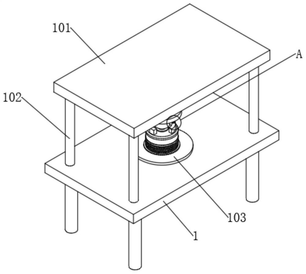
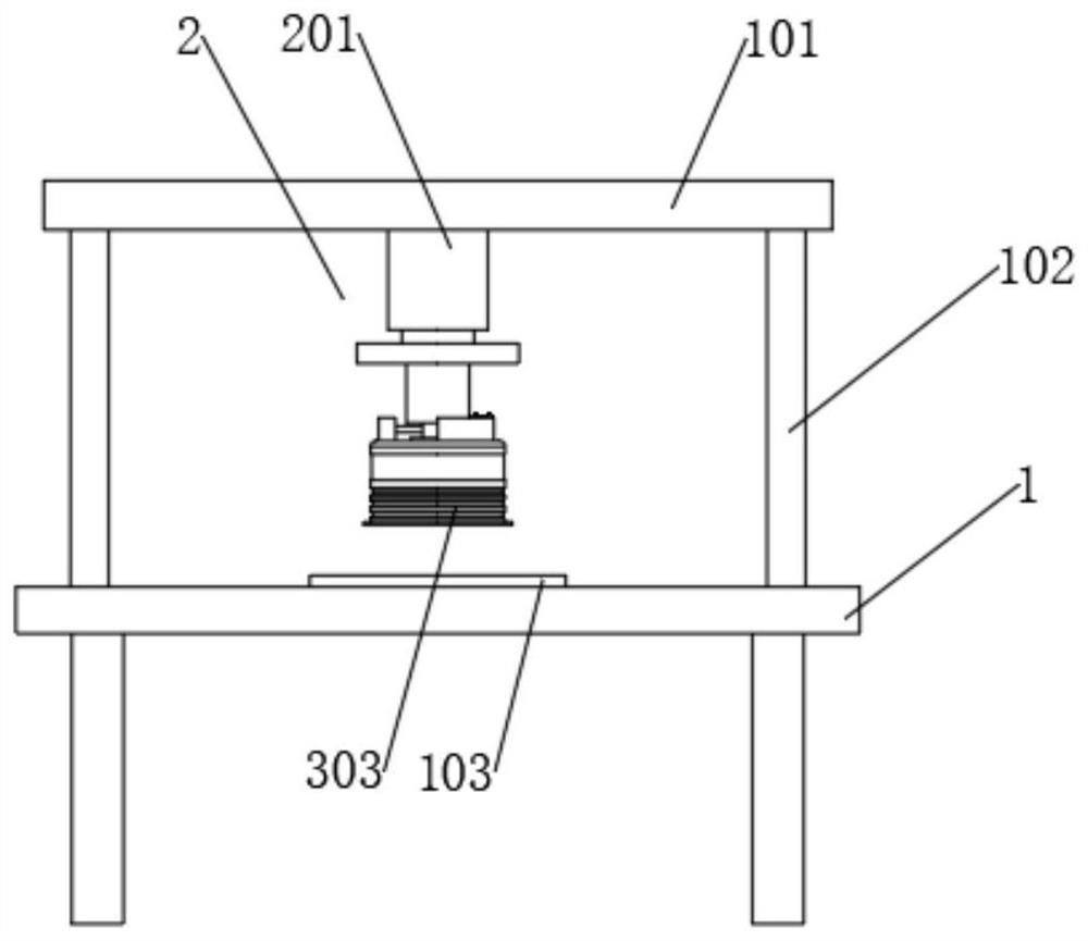
[0046] The invention discloses an environment-friendly production equipment for semiconductor materials, refer to Figure 1-Figure 8 As shown, it includes a workbench 1 , a polishing mechanism 2 , a sealing positioning mechanism 3 , and a dust suction mechanism 4 .

[0047] The upper side of the worktable 1 is provided with an upper plate 101 , and the upper plate 101 is used for installing the polishing mechanism 2 .

[0048] In addition, a plurality of connecting columns 102 are connected between the worktable 1 and the upper plate 101 , and a polishing plate 103 is installed on the worktable 1 , an...


PUM


Abstract

The invention discloses environment-friendly production equipment for a semiconductor material and a using method of the environment-friendly production equipment. The environment-friendly production equipment comprises a workbench, a polishing mechanism, a sealing and positioning mechanism and a dust collection mechanism. An upper plate is arranged on the upper side of the workbench, a plurality of connecting columns are connected between the workbench and the upper plate, and a polishing plate is installed on the workbench; the polishing mechanism is mounted on the lower bottom surface of the upper plate and is used for polishing the wafer; the sealing and positioning mechanism is arranged on the outer side of the polishing mechanism and used for positioning and sealing the wafer, flying dust generated when the wafer is polished is prevented from overflowing, and the sealing and positioning mechanism comprises a sealing cover. Through the arrangement of the corresponding mechanisms, wafers can be positioned, manual positioning of workers is avoided, the safety of the workers can be guaranteed, in addition, flying dust generated in the wafer polishing process can be collected and treated, floating of the flying dust is avoided, the probability that the workers inhale the flying dust is greatly reduced, and the working efficiency is improved. And the body health of workers can be ensured to a certain extent.

Description

technical field [0001] The invention belongs to the technical field of semiconductor materials, and in particular relates to an environment-friendly production equipment for semiconductor materials and a use method thereof. Background technique [0002] Semiconductor materials are a class of electronic materials with semiconductor properties (conductivity between conductors and insulators, resistivity in the range of about 1mΩ·cm-1GΩ·cm), which can be used to make semiconductor devices and integrated circuits. Semiconductor materials are widely used in integrated circuits, consumer electronics, communication systems, photovoltaic power generation, lighting, high-power power conversion and other fields. [0003] The main processing process of semiconductor products is divided into wafer manufacturing and packaging testing. Among them, wafer manufacturing includes 7 processes of diffusion, lithography, etching, ion implantation, thin film growth, polishing and metallization. ...

Claims


Application Information

Patent Timeline
Patent Type & Authority Applications(China)
IPC IPC(8): B24B29/02B24B41/04B24B41/06B24B47/12B24B47/22B24B55/04B24B55/06B24B55/12
CPCB24B29/02B24B41/04B24B41/06B24B47/22B24B47/12B24B55/04B24B55/06B24B55/12Y02P70/50
Inventor 朱春李述周
Owner 江苏科沛达半导体科技有限公司
Why Eureka
Try Eureka