Semiconductor structure and forming method thereof

A technology of semiconductor and channel structure, which is applied in the direction of semiconductor devices, semiconductor/solid-state device manufacturing, electrical components, etc., can solve the problems that the performance of fully surrounded gate transistors needs to be improved, so as to improve the increase of gate resistance and increase the circuit speed , the effect of performance improvement

Pending Publication Date: 2022-08-09
SEMICON TECH INNOVATION CENT(BEIJING) CORP
View PDF0 Cites 0 Cited by
  • Summary
  • Abstract
  • Description
  • Claims
  • Application Information

AI Technical Summary

Problems solved by technology

[0004] However, the performance of current all-around gate transistors still needs to be improved

Method used


Image

  • Semiconductor structure and forming method thereof
  • Semiconductor structure and forming method thereof
  • Semiconductor structure and forming method thereof

Examples


Embodiment Construction

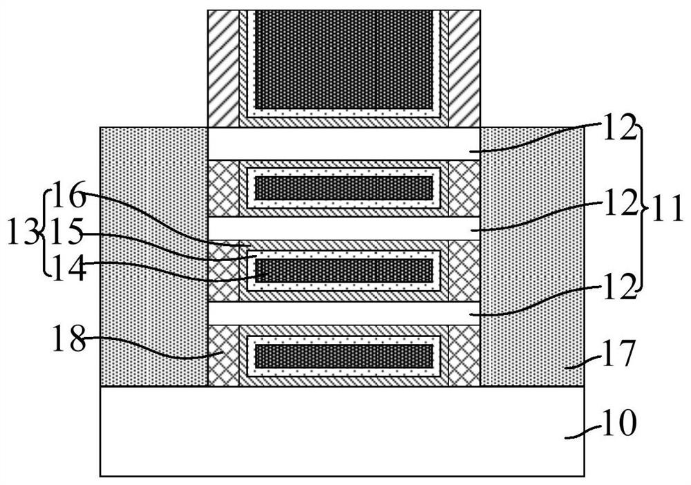
[0015] It can be known from the background art that the performance of the current fully surrounded gate transistor needs to be improved. The reason why the performance of the semiconductor structure needs to be improved is now analyzed in combination with a semiconductor structure. figure 1 It is a schematic diagram of a semiconductor structure.

[0016] The semiconductor structure includes: a substrate 10; a channel structure layer 11 located on the substrate 10 and spaced from the substrate 10; the channel structure layer 11 includes one or more spaced channel layers 12; source and drain doped layers 17 , located on both sides of the channel structure layer 11 along the length of the channel layer 12 and covering the sidewalls of the channel structure layer 11 , the source-drain doped layer 17 and the adjacent channel layer, or the source-drain doped layer 17 The substrate 10 and the channel layer 12 adjacent to the substrate 10 form a through groove (not marked); the inne...


PUM


Abstract

The invention discloses a semiconductor structure and a forming method thereof. The semiconductor structure comprises a channel structure layer; the source-drain doping layers are located on the two sides of the channel structure layer in the length direction of the channel layers, and the source-drain doping layers and the adjacent channel layers or the source-drain doping layers, the substrate and the channel layers adjacent to the substrate define through grooves; the grid opening is communicated with the through groove, is positioned between the source-drain doping layers and stretches across the channel structure layer; the gate structure is filled in the gate opening and the through groove and comprises a gate function layer surrounding the channel layer and a gate electrode layer which is located on the gate function layer and fills the gate opening and the through groove, the gate function layer exposes the through groove and the side wall of the gate opening, and the gate electrode layer is in contact with the gate opening and the side wall of the through groove. According to the embodiment of the invention, the gate function layer exposes the gate opening and the side wall of the through groove, a larger filling space can be provided for the gate electrode layer, the proportion of the gate electrode layer to the volume of the gate structure is increased, and the problem that the gate resistance is increased due to the reduction of the gate length is solved.

Description

technical field [0001] Embodiments of the present invention relate to the field of semiconductor manufacturing, and in particular, to a semiconductor structure and a method for forming the same. Background technique [0002] With the rapid development of semiconductor manufacturing technology, semiconductor devices are developing in the direction of higher component density and higher integration, and the development trend of semiconductor process nodes following Moore's Law is decreasing. As the most basic semiconductor device, transistors are currently being widely used. Therefore, with the increase in the component density and integration of semiconductor devices, the channel length of transistors has to be continuously shortened in order to adapt to the reduction of process nodes. [0003] In order to better meet the requirement of scaling down the device size, the semiconductor process gradually begins to transition from planar transistors to three-dimensional transisto...

Claims


Application Information

Patent Timeline
Patent Type & Authority Applications(China)
IPC IPC(8): H01L29/78H01L29/423H01L21/336
CPCH01L29/66795H01L29/785H01L29/42356
Inventor 武咏琴卜伟海
Owner SEMICON TECH INNOVATION CENT(BEIJING) CORP
Why Eureka
Try Eureka