
Photon crystal wavelength division mutiplex device

A technology of wavelength division multiplexing devices and photonic crystals, applied in the coupling of optical waveguides, electrical components, electromagnetic wave transmission systems, etc., can solve problems such as design and manufacturing complexity, achieve time reduction, optimization process reduction, and increase the number of channels Effect

Inactive Publication Date: 2005-01-12
INST OF PHYSICS - CHINESE ACAD OF SCI
View PDF0 Cites 2 Cited by
  • Summary
  • Abstract
  • Description
  • Claims
  • Application Information

AI Technical Summary

Problems solved by technology

However, there are disadvantages in this process of wave resolution by channel downtunneling: in order to make the frequency in waveguide 1 be f 1 The light completely tunnels into the waveguide 2, and the coupling unit used for the tunneling process must contain more than two cavities to achieve high tunneling efficiency, which makes the design and manufacture of the entire system very complicated

Method used


Image

  • Photon crystal wavelength division mutiplex device
  • Photon crystal wavelength division mutiplex device
  • Photon crystal wavelength division mutiplex device

Examples


Embodiment 1

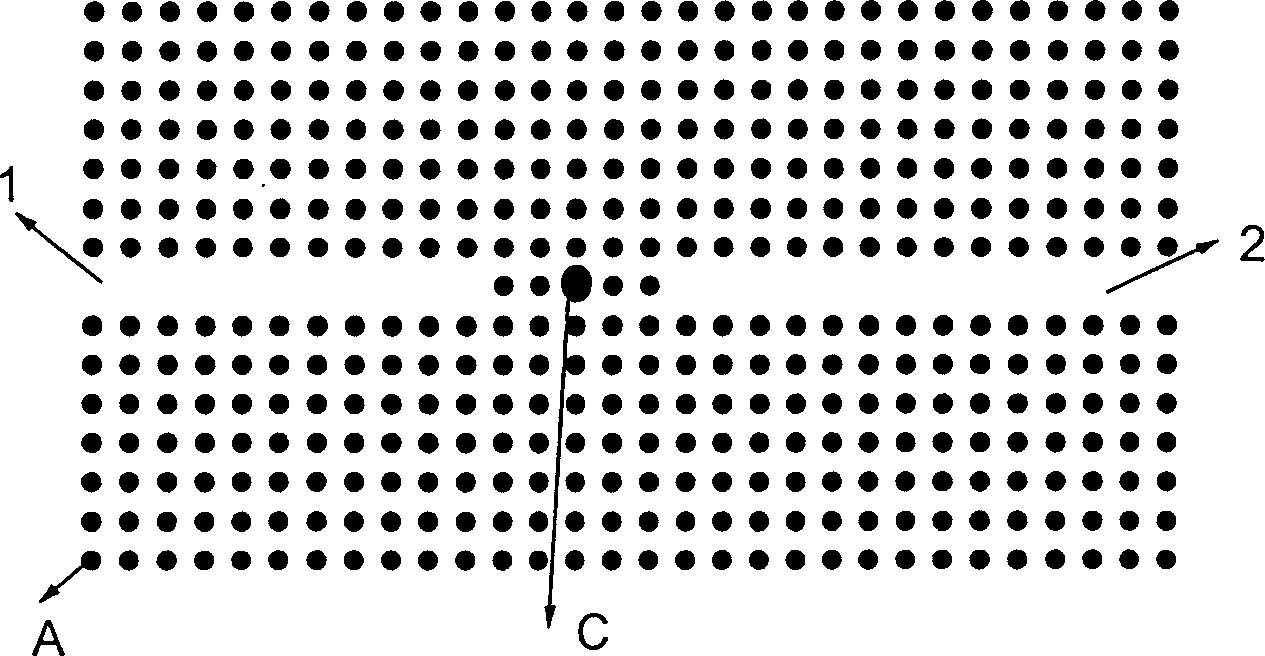
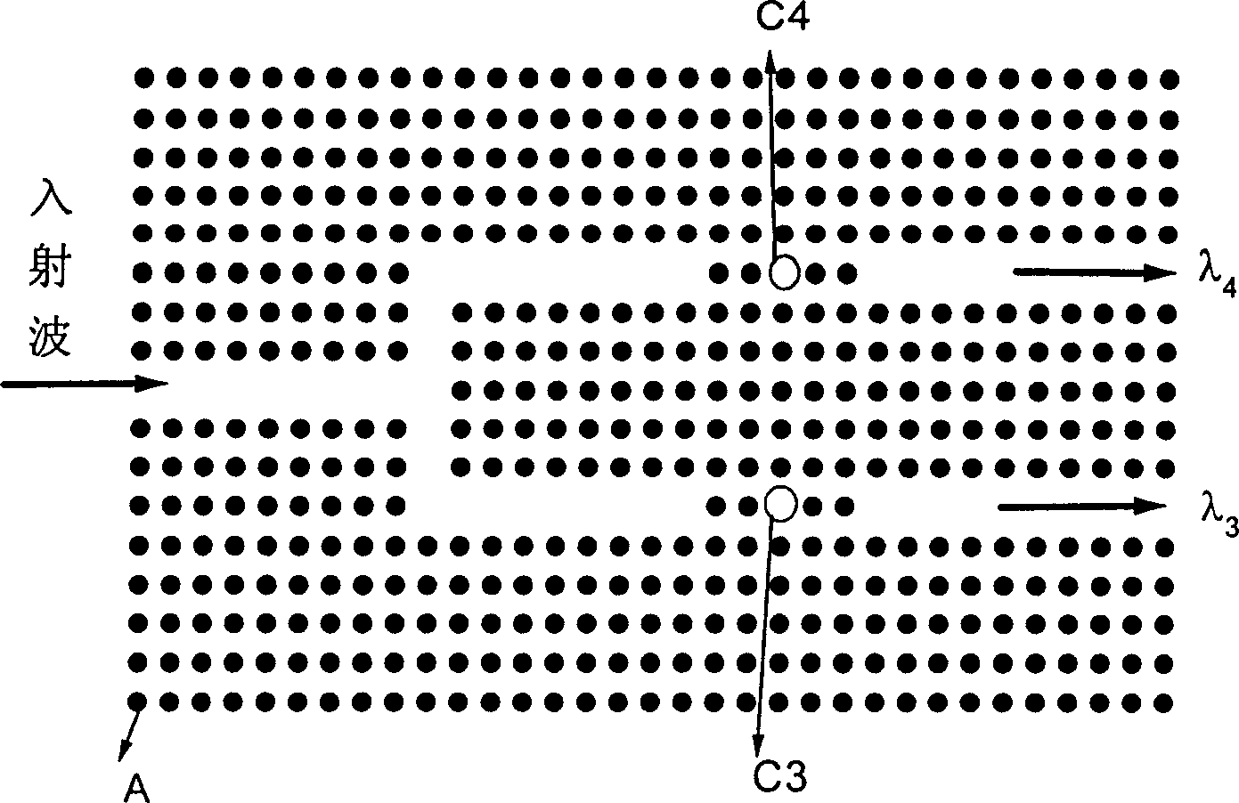
[0025] image 3 It is a device for wave resolution with two channels, where A represents the dielectric cylinder "atom" that constitutes a two-dimensional photonic crystal; C3 and C4 are introduced defects (microcavities). The wavelengths of the defect modes introduced by these defects are λ 3 and lambda 4 . When the wavelengths are λ 3 and lambda 4 When the incident wave enters the photonic crystal along the photonic crystal waveguide, it undergoes resonant coupling with C3 and C4, λ 3 and lambda 4 It comes out from the lower and upper waveguide ports respectively, which completes the function of separating different frequencies. This is the simplest photonic crystal wave resolution device. The two optical paths are symmetrical, that is, the path from the defect to the entrance of the light wave is consistent. Respectively image 3 and Figure 4 When a line of light source is placed at the entrance of the waveguide, the light wave will be coupled into the waveguide,...

Embodiment 2

[0027] Figure 8 It is a structural schematic diagram of a device for wave resolution with 4 channels, similar to Embodiment 1, it can also separate light waves of 4 different frequency bands. where C7, C8, C9 and C10 are introduced defects, and their defect modes correspond to λ 7 , lambda 8 , lambda 9 and lambda 10 . In two dimensions, this photonic crystal is a square photonic crystal. The black dots in it represent a dielectric cylinder, while the surroundings represent another dielectric cylinder. The radius of the dielectric cylinder is chosen to be 0.1858 times the lattice constant, the dielectric constant is 8.4, and the dielectric constant of the surrounding medium is 1.04. The radii of the dielectric cylinders of the four introduced defects C7, C8, C9, and C10 are all 0.3545 times the lattice constant, and the dielectric constants are 5.7, 6.5, 7.0, and 4.5, respectively. Using the multiple scattering method, one can get Figure 9 The wave solution is shown w...

Embodiment 3

[0029] Design a device for wave resolution with 16 channels (such as Figure 10 As shown), 16 symmetrical defects constitute 16 channels for symmetrical wave resolution. Among them, C11, C12, C13, ..., C26 are different defects, forming 16 defect states, and the center frequencies of these defect states are λ 11 , lambda 12 , lambda 13 ,...,λ 26 . In this way, 16 signals of different frequencies can be detected from the outlet. The structure can be two-dimensional or three-dimensional, and can be easily expanded to 32, 64 or even more channels. Moreover, the structural design is very simple, that is, the principle of symmetry is followed, so that the direct coupling efficiency of all channels is the highest.


PUM


Abstract

This invention relates to a WDM apparatus of microwave and light wave, especially relates to light wave demultiple and multiplex apparatus. By leading-in defect and microcavity in 2-D or 3-D photonic crystals, this invention uses the resonant coupling action of the microcavlty and symmetric optical path design to increase the available efficiency of the apparatus. Designs of this invention is simple with shorter simulation and option time and easy to increase channel numbers of WDM.

Description

technical field [0001] The invention relates to a microwave and light wave wavelength division multiplexing device, in particular to a light wave decomposing and wave multiplexing device. Background technique [0002] In optical fiber communication, the optical fiber can transmit signals in a very wide frequency range, so how to couple the light of different signals carried by different frequencies into an optical fiber, and how to extract the signals carried by the waves of different frequencies transmitted by the optical fiber, are It has become an important research direction to expand the capacity of optical fiber communication, that is, the so-called wavelength division multiplexing technology. [0003] Photonic crystals are artificial crystals formed by periodic arrangement of two or more media. There is a photonic band gap in the photonic band structure of the photonic crystal. When the frequency of the photon is within the photonic band gap, the photon cannot propag...

Claims


Application Information

Patent Timeline
IPC IPC(8): G02B6/24
Inventor 金崇君程丙英张道中
Owner INST OF PHYSICS - CHINESE ACAD OF SCI
Features
  • Generate Ideas
  • Intellectual Property
  • Life Sciences
  • Materials
  • Tech Scout
  • Unparalleled Data Quality
  • Higher Quality Content
  • 60% Fewer Hallucinations
Learn More