Semiconductor substrate, field effect transistor, and method for forming silicon germanide layer

A field-effect transistor and semiconductor technology, which is applied in the manufacture of semiconductor/solid-state devices, semiconductor devices, electrical components, etc., can solve the problems of increased penetration dislocation density, reduction of dislocation, and deterioration of surface roughness, etc., and achieve high yield.

Inactive Publication Date: 2005-08-24
SUMCO CORP
View PDF4 Cites 2 Cited by
  • Summary
  • Abstract
  • Description
  • Claims
  • Application Information

AI Technical Summary

Problems solved by technology

[0007] For example, in the case of using a buffer layer in which the composition ratio of Ge is changed, although the threading dislocation density can be greatly reduced, there is a disadvantage in that the surface roughness is deteriorated. In this case, although the surface roughness can be greatly

Method used


Image

  • Semiconductor substrate, field effect transistor, and method for forming silicon germanide layer
  • Semiconductor substrate, field effect transistor, and method for forming silicon germanide layer
  • Semiconductor substrate, field effect transistor, and method for forming silicon germanide layer

Examples


Embodiment Construction

[0044] Below, refer to Figure 1 to Figure 6 , While explaining the first embodiment of the present invention.

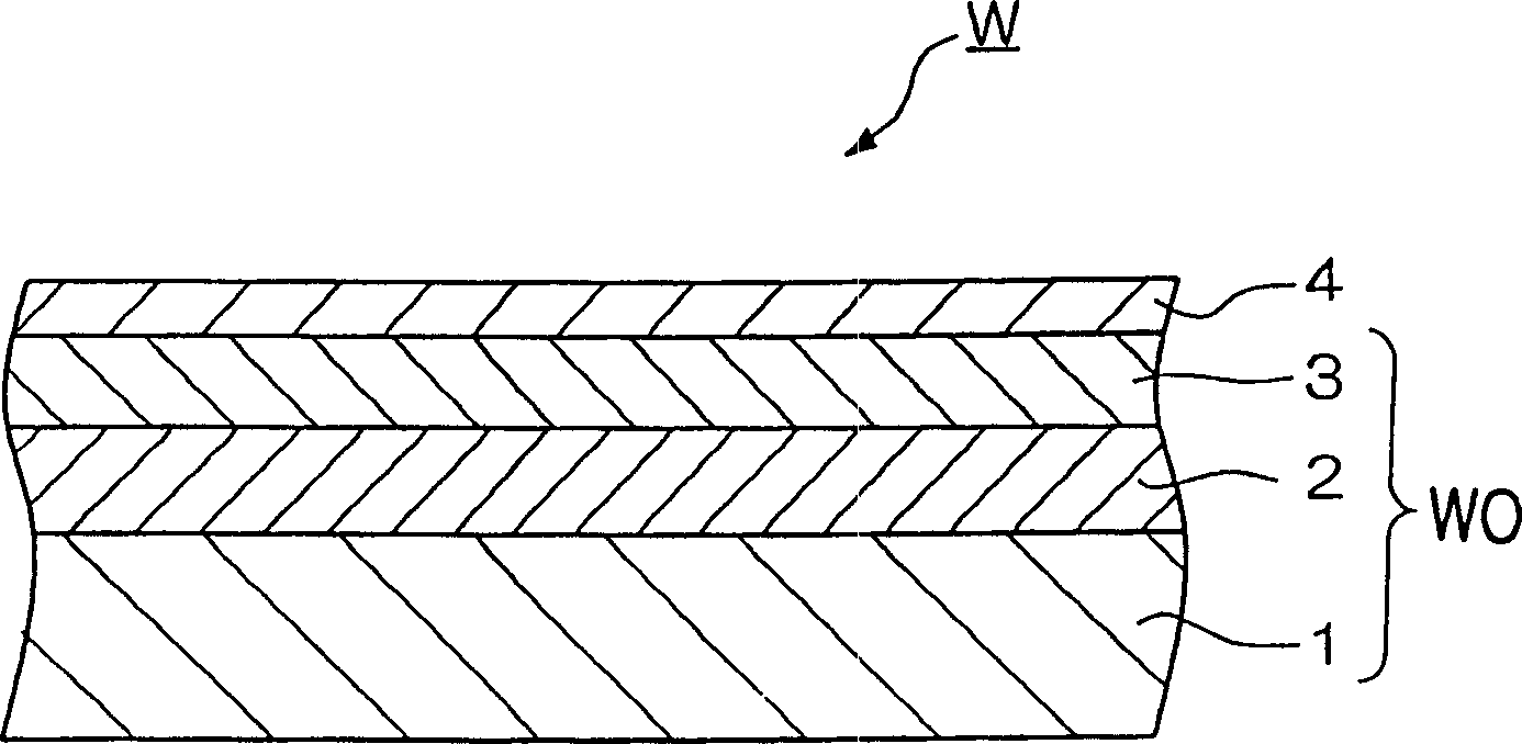
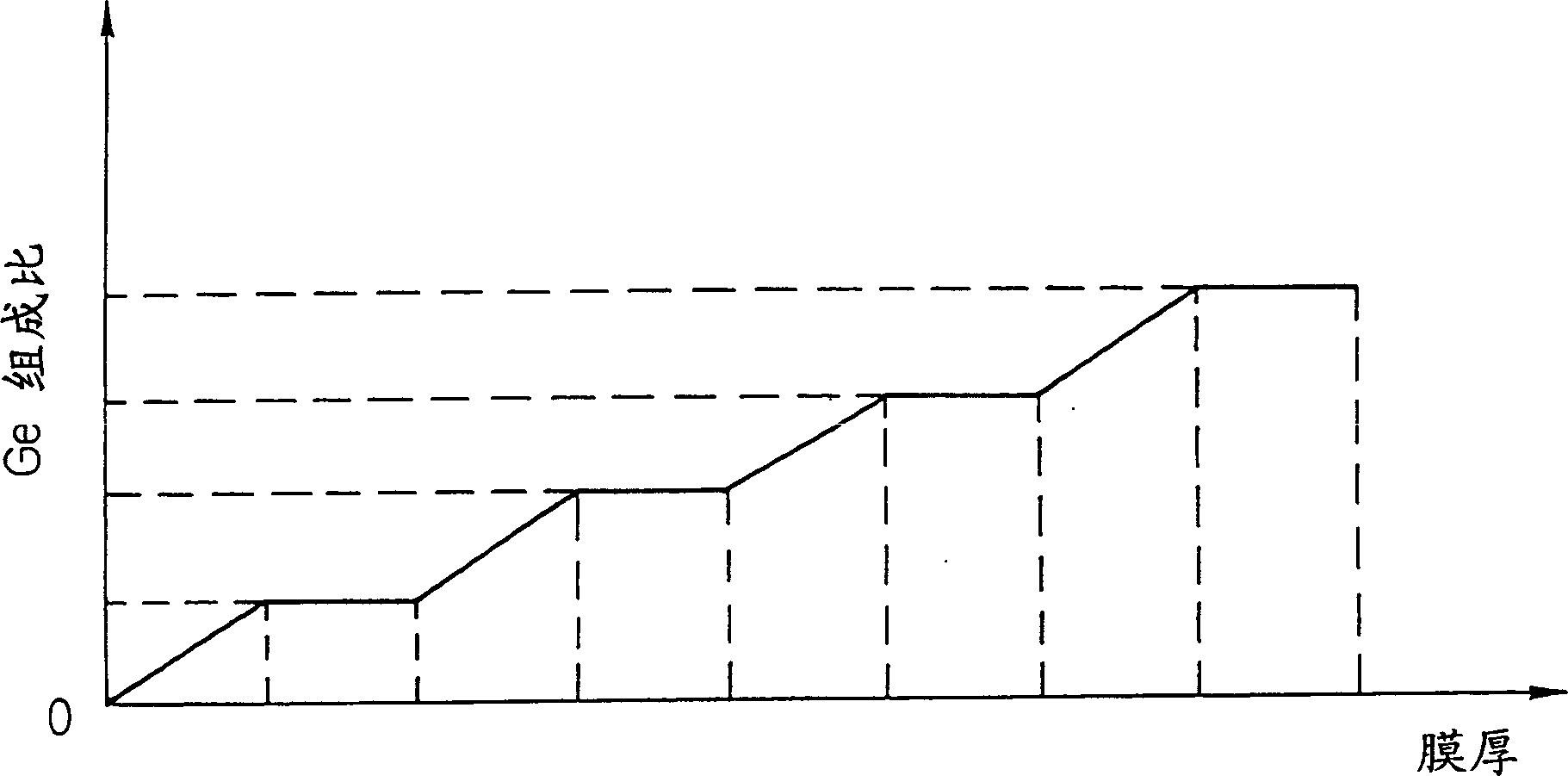
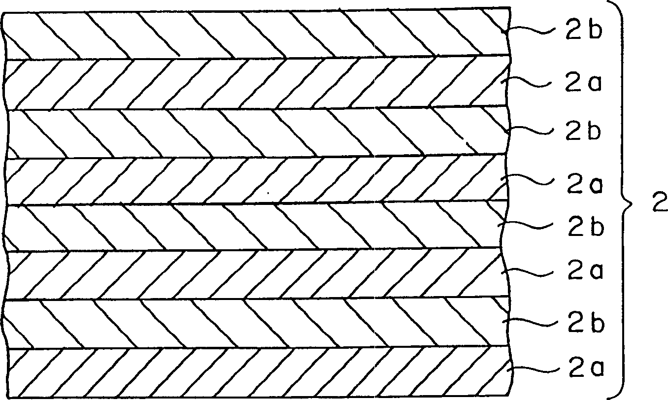
[0045] figure 1 The cross-sectional structure of the semiconductor wafer (semiconductor substrate) W provided with the semiconductor wafer (semiconductor substrate) WO of the present invention and the deformed Si layer is shown in FIG. figure 1 As shown in the low-pressure CVD method, the Ge composition ratio x from 0 to y (for example, y=0.3) on the Si substrate 1 manufactured by the upward growth of the CZ method has an inclination in the film formation direction and is stepped Morphological changes of Si 1-x Ge x The step gradient layer (SiGe buffer layer) 2 is epitaxially grown. In addition, in the film formation by the above-mentioned low-pressure CVD method, H 2 As a carrier gas, SiH is used 4 And GeH 4 As the source gas.

[0046] Secondly, epitaxially grow Si with a certain Ge composition ratio on the stepped inclined layer 2. 1-y Ge y The relaxation layer 3 to...


PUM


Abstract

A semiconductor substrate, a field effect transistor, a method of forming a SiGe layer and a method of forming a strained Si layer using the same, and a method of manufacturing a field effect transistor are provided, which enable the threading dislocation density of the SiGe layer to be reduced and the surface roughness to be minimized. On top of a Si substrate 1 is provided a SiGe buffer layer 2, 12 constructed of a plurality of laminated layers comprising alternating layers of a SiGe gradient composition layer 2a, 12a in which the Ge composition ratio increases gradually from the Ge composition ratio of the base material, and a SiGe constant composition layer 2b, 12b which is provided on top of the gradient composition layer and in which the Ge composition ratio is equal to that of the upper surface of the gradient composition layer.

Description

Technical field [0001] The present invention relates to a method for forming a SiGe layer suitable for forming semiconductor substrates, field effect transistors, and deformed Si layers used in high-speed MOSFETs and the like, and a method for forming a deformed Si layer and a method for manufacturing a field effect transistor using the method. Background technique [0002] In recent years, high-speed MOSFETs, MODFETs, and HEMTs using a deformed Si layer epitaxially grown on a Si (silicon) wafer via a SiGe (silicon germanium) layer as a channel region have been proposed. In this deformed Si-FET, SiGe, which has a larger lattice constant than Si, generates tensile deformation in the Si layer. Therefore, the band structure of Si is changed to release degeneracy, and carrier mobility is improved. Therefore, by using this deformed Si layer as a channel region, it is possible to achieve a speed increase of about 1.5 to 8 times that of normal. In addition, a normal Si substrate using t...

Claims


Application Information

Patent Timeline
IPC IPC(8): H01L29/78H01L21/20H01L21/205H01L21/335H01L21/337H01L21/338H01L29/10H01L29/778H01L29/812H01L31/04
CPCH01L21/0251H01L21/0245H01L21/02532H01L29/66916H01L21/02505H01L29/1054H01L21/02381H01L21/18
Inventor 水嶋一树盐野一郎山口健志
Owner SUMCO CORP
Why Eureka
Try Eureka