Method for manufacturing semiconductor device

a manufacturing method and semiconductor technology, applied in the direction of semiconductor devices, basic electric elements, electrical appliances, etc., can solve the problems of glass substrate shrinkage, yield decline, and decrease of bonding strength between single-crystal silicon layers, and achieve high yield

Inactive Publication Date: 2008-11-13
SEMICON ENERGY LAB CO LTD
View PDF15 Cites 15 Cited by
  • Summary
  • Abstract
  • Description
  • Claims
  • Application Information

AI Technical Summary

Benefits of technology

[0008]In view of such a problem, it is an object of the present invention to provide a method for manufacturing, with high yield, a semiconductor device having a crystalline semiconductor layer that can be used in practical applications even if a substrate with low upper temperature limit, such as a glass substrate, is used.
[0010]Before heat treatment for separation of a semiconductor substrate, a groove is formed in a part of the semiconductor substrate to form an isolated projecting portion. After that, the projecting portion is bonded to a supporting substrate, and the heat treatment for separation of the semiconductor substrate is performed. Because the supporting substrate shrinks due to the heat treatment for separation of the semiconductor substrate, the position of an SOI layer that is bonded to the supporting substrate also changes and distortion stress is generated. However, because the projecting portion is isolated by the groove, the projecting portion is not continuously bonded to the supporting substrate and is isolated. The generation of distortion stress on a semiconductor layer due to the shrinkage of the supporting substrate can be suppressed, and film separation and a decrease of bonding strength between the bonding surfaces can be reduced. In addition, because the shrinkage of the supporting substrate does not tend to occur easily in a later heating step, the misalignment of photomasks in a plurality of photolithography steps can be suppressed.
[0017]After a groove is formed in a part of a semiconductor substrate to form a semiconductor substrate that has a projecting portion, the protecting portion can be bonded to a supporting substrate; the semiconductor substrate can be separated from a brittle region by heat treatment; and an SOI layer can be provided over the supporting substrate. Because the projecting portion on the semiconductor substrate is isolated, the separation of the SOI layer that accompanies the shrinkage of the supporting substrate due to heating can be prevented.
[0019]Therefore, by use of the SOI layer, a semiconductor device can be manufactured with high yield.

Problems solved by technology

Therefore, in the case where an SOI substrate is formed by bonding of single-crystal silicon to a glass substrate that has an upper temperature limit of about 700° C., which is used for a liquid crystal panel or the like in order to lower the substrate cost, there arises a problem in that a glass substrate shrinks when heat treatment at such a high temperature is performed.
The shrinkage of a glass substrate results in a decrease of bonding strength between a single-crystal silicon layer and the glass substrate, and a decrease of yield.
Because the supporting substrate shrinks due to the heat treatment for separation of the semiconductor substrate, the position of an SOI layer that is bonded to the supporting substrate also changes and distortion stress is generated.

Method used


Image

  • Method for manufacturing semiconductor device
  • Method for manufacturing semiconductor device
  • Method for manufacturing semiconductor device

Examples


embodiment mode 1

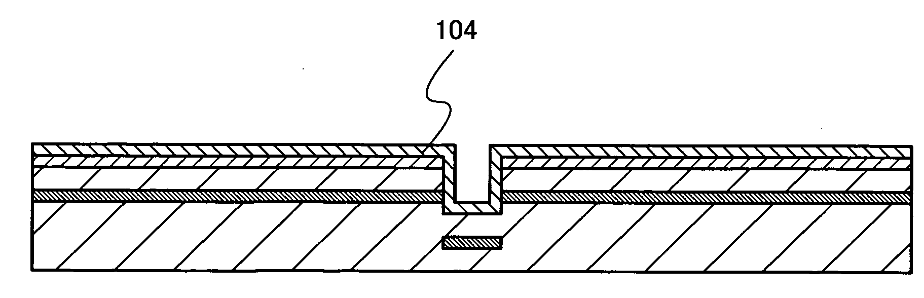
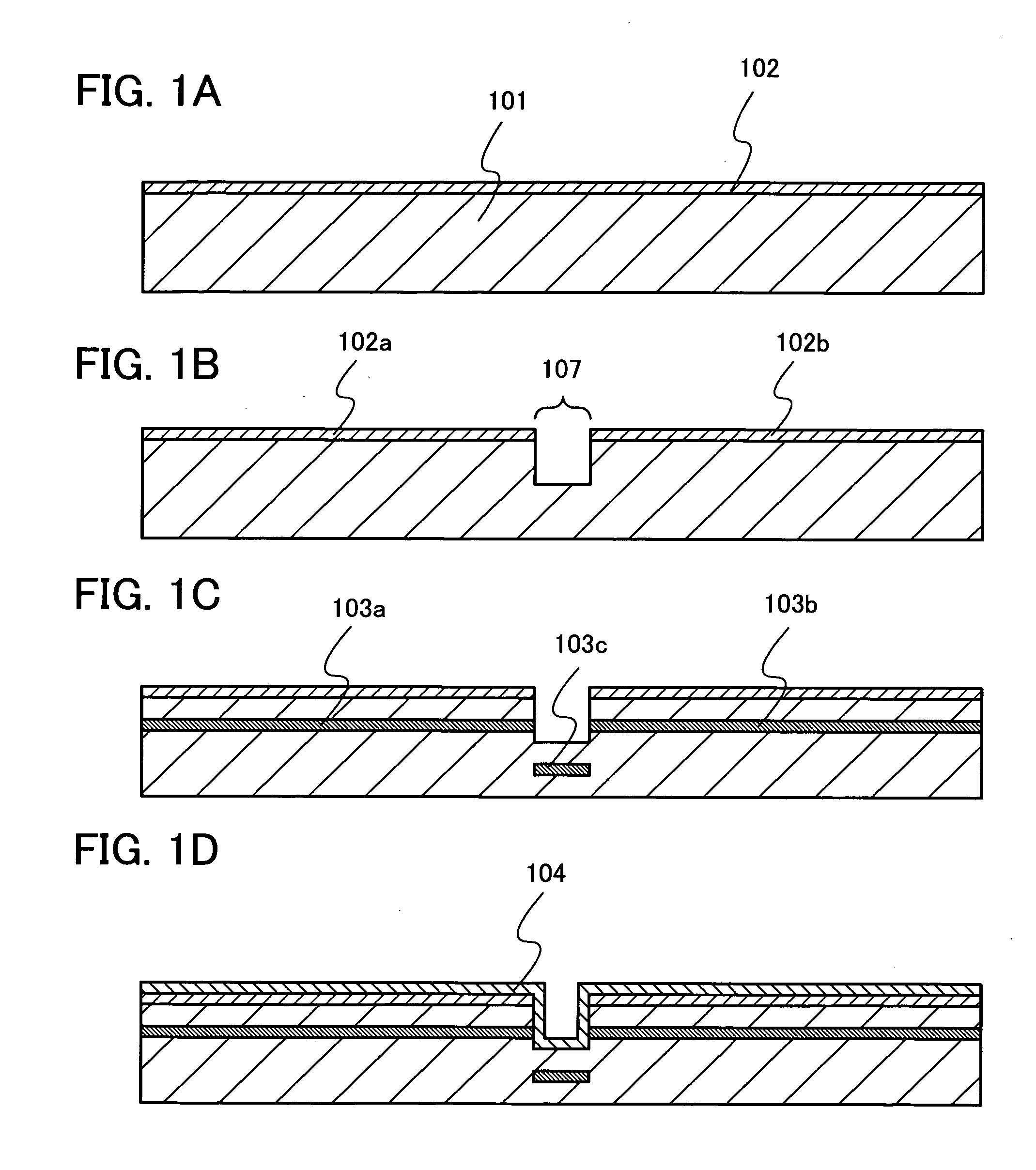
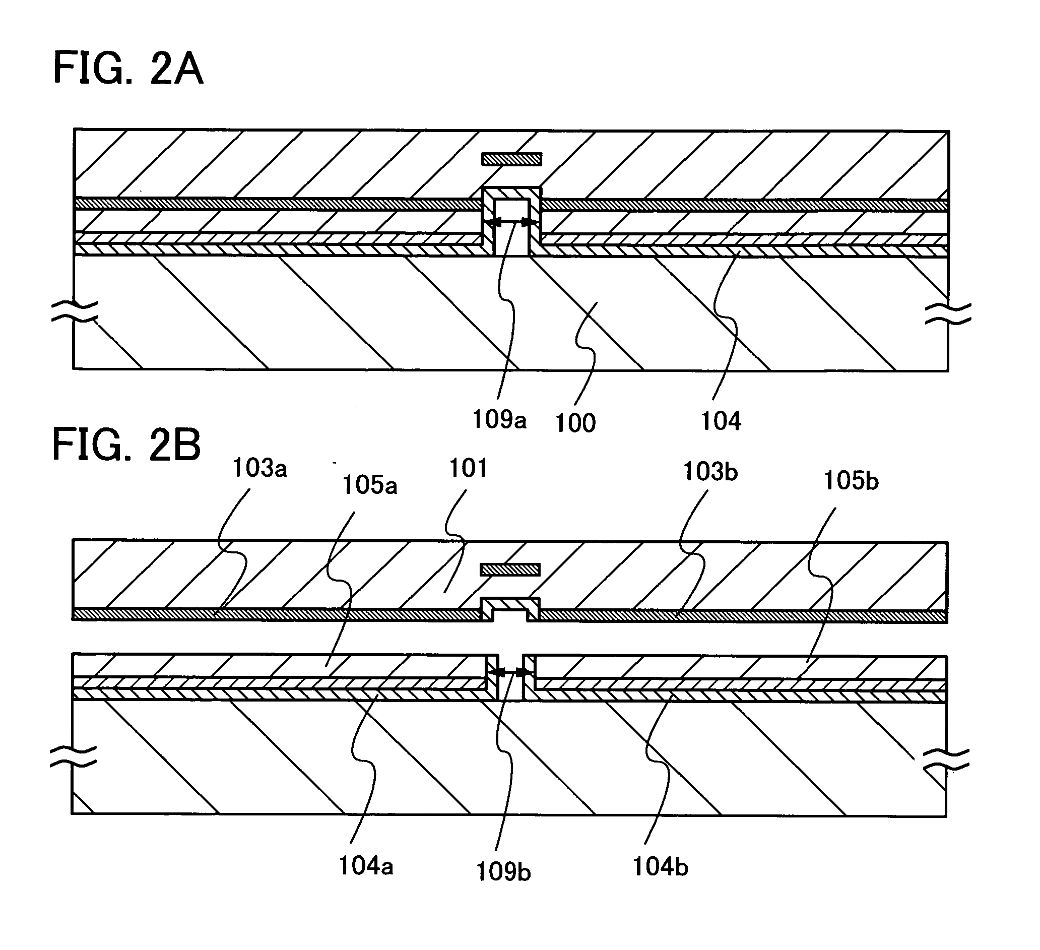
[0052]In this embodiment mode, a method for manufacturing a semiconductor device with high yield, in consideration of the shrinkage of a supporting substrate in bonding a semiconductor substrate to the supporting substrate and performing heat treatment to separate a part of the semiconductor substrate, is described with reference to FIGS. 1A to 7. FIG. 1A to 4B are cross-sectional views of FIGS. 5 to 7 along A-B. FIG. 5 shows a top view of a semiconductor substrate, and FIGS. 6 and 7 show top views of a supporting substrate.

[0053]In FIG. 1A, as a semiconductor substrate 101, a crystalline semiconductor substrate or a single-crystal semiconductor substrate can be used. Examples of a crystalline semiconductor substrate or a single-crystal semiconductor substrate include a silicon substrate, a germanium substrate, and the like, and alternatively, a substrate of a compound semiconductor such as silicon germanium, gallium arsenide, or indium phosphide can be used. Commercial silicon subs...

embodiment mode 2

[0105]A method for manufacturing a semiconductor device, which is different from that in the above mode, is described with reference to FIGS. 8A to 10C. Here, manufacture of a semiconductor device, by which a semiconductor substrate can be bonded to a supporting substrate with high yield, is described.

[0106]As shown in FIG. 8A, degreasing cleaning is performed on the surface of a semiconductor substrate 101; an oxide film on the surface is removed; and thermal oxidation is performed. As thermal oxidation, general dry oxidation may be performed; however, oxidation in an oxidizing atmosphere to which a halogen is added is preferably performed. For example, heat treatment is performed at a temperature of 700° C. or higher in an atmosphere which contains HCl at 0.5 volume % to 10 volume % (preferably, 3 volume %) with respect to oxygen. The thermal oxidation is preferably performed at a temperature of 950° C. to 1100° C. The processing time may be 0.1 hours to 6 hours, preferably, 0.5 h...

embodiment mode 3

[0129]A method for manufacturing a semiconductor device, which is different from that in the above mode, is described with reference to FIGS. 21A to 21C. Here, manufacture of a semiconductor device, by which a semiconductor substrate can be bonded to a supporting substrate with high yield, is described.

[0130]In a similar manner to Embodiment Mode 2, as shown in FIG. 21A, degreasing cleaning is performed on the surface of a semiconductor substrate 101; an oxide film on the surface is removed; and then, thermal oxidation is performed to form an oxide layer 111 on the surface of the semiconductor substrate 101. Here, by oxidation in an oxidizing atmosphere into which a halogen is introduced, gettering of a metal impurity by a halogen element is performed to compensate defects at the interface between the semiconductor substrate 101 and the oxide layer 111 and to lower local level density at the interface.

[0131]Next, in a similar manner to Embodiment Mode 2, a blocking layer 102 may be ...


PUM


Abstract

An object is to provide a method for manufacturing, with high yield, a semiconductor device having a crystalline semiconductor layer even if a substrate with low upper temperature limit. A groove is formed in a part of a semiconductor substrate to form a semiconductor substrate that has a projecting portion, and a bonding layer is formed to cover the projecting portion. In addition, before the bonding layer is formed, a portion of the semiconductor substrate to be the projecting portion is irradiated with accelerated ions to form a brittle layer. After the bonding layer and the supporting substrate are bonded together, heat treatment for separation of the semiconductor substrate is performed to provide a semiconductor layer over the supporting substrate. The semiconductor layer is selectively etched, and a semiconductor element is formed and a semiconductor device is manufactured.

Description

BACKGROUND OF THE INVENTION[0001]1. Field of the Invention[0002]The present invention relates to a method for manufacturing a semiconductor device using a substrate that has an SOI structure.[0003]2. Description of the Related Art[0004]Instead of silicon wafers that are manufactured by thinly cutting an ingot of a single-crystal semiconductor, semiconductor substrates called silicon-on-insulator (SOI) substrates have been developed, which have a thin single-crystal semiconductor layer over an insulating layer. When transistors that are to be included in an integrated circuit are formed using an SOI substrate, parasitic capacitance between drains of the transistors and the substrate can be reduced, which is considered to be effective in improving operation speed and in reducing the amount of power consumption. Therefore, SOI substrates are expected to be applied to high-performance semiconductor devices such as microprocessors.[0005]As a method for manufacturing SOI substrates, a hyd...

Claims


Application Information

Patent Timeline
Patent Type & Authority Applications(United States)
IPC IPC(8): H01L21/76
CPCH01L21/3081H01L21/76254H01L29/66772H01L27/1266H01L27/1214H01L21/76259
Inventor YAMAZAKI, SHUNPEIOHNUMA, HIDETO
Owner SEMICON ENERGY LAB CO LTD
Why Eureka
Try Eureka