Electro-optical device and electronic apparatus

Active Publication Date: 2014-10-02
SEIKO EPSON CORP
View PDF13 Cites 16 Cited by
  • Summary
  • Abstract
  • Description
  • Claims
  • Application Information

AI Technical Summary

Benefits of technology

[0009]According to an aspect of the invention, an electro-optical device includes a first substrate, a second substrate, an electro-optical substance disposed between the substrates, a sealing material disposed in the spacing between the first substrate and the second substrate and surrounding the periphery of the electro-optical substance, a moistureproof resin layer disposed outside of the sealing material and having a portion located in the spacing, and an gap region defined in at least a portion of the space between the sealing material and the moistureproof resin layer.
[0010]According to the electro-optical device in one aspect of the invention, the gap region disposed between the sealing material surrounding the periphery of the electro-optical substance and the moistureproof resin layer can trap a gas generated from the resin component such as the moistureproof resin layer or the sealing material and can thereby suppress the generation of bubbles in the electro-optical substance. Further, uncured components or nonvolatile impurities eluted from the moistureproof resin layer can also be trapped in the gap region. Thus, the electro-optical substance, for example, a liquid crystal, can be suppressed from misalignment by the influence of outgassing and impurities.
[0011]In the above aspect of the invention, the electro-optical device preferably includes an inorganic film layer disposed outside of the moistureproof resin layer and at least partially in contact with the outer surface of the moistureproof resin layer. In this case in which the inorganic film layer is further disposed outside of the moistureproof resin layer, the moistureproof resin layer may be formed in such a manner that the moistureproof resin impregnates the spacing between the pair of substrates to facilitate the formation of the inorganic film layer. Thus, the inorganic film layer disposed on the outer surface of the moistureproof resin layer provides higher moisture proofness than obtained with the moistureproof resin layer alone.
[001

Problems solved by technology

However, reducing this distance results in a problem that the moisture proofness of the seal is deteriorated.
In detail, when such liquid crystal devices are used in hot and humid environments, water in the air may penetrate the liquid crystal through the sealing material and may adversely affect the alignment of the liquid crystal.
Any changes in the alignment of liquid crystal cause display defects such as uneven brightness.
Although the liquid crystal device disclosed in JP-A-2009-163082 achieves improved moisture proofness by the configuration in which the inorganic gas barrier layer is disposed on the outer surface of the gas barrier member formed of a moistureproof resin, the application of heat to the liquid crystal device during the formation of the inorganic gas barrier layer causes the occurrence of outgassing or the elution of impurities from the resinous sealing material and g

Method used


Image

  • Electro-optical device and electronic apparatus
  • Electro-optical device and electronic apparatus
  • Electro-optical device and electronic apparatus

Examples


first embodiment

A: First Embodiment

Configuration of Liquid Crystal Device

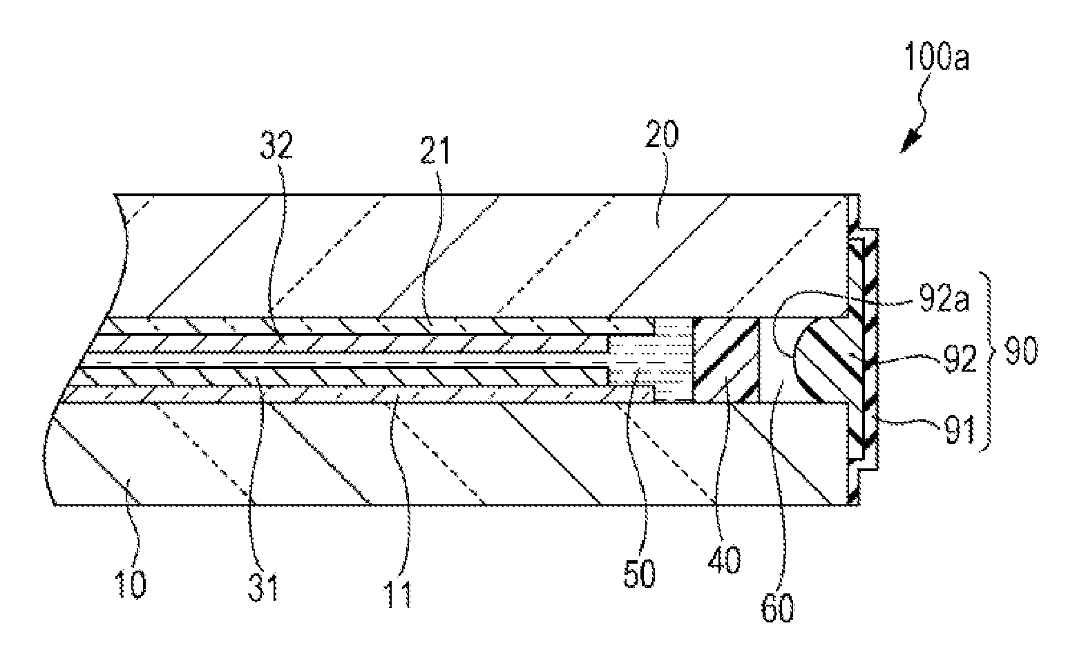
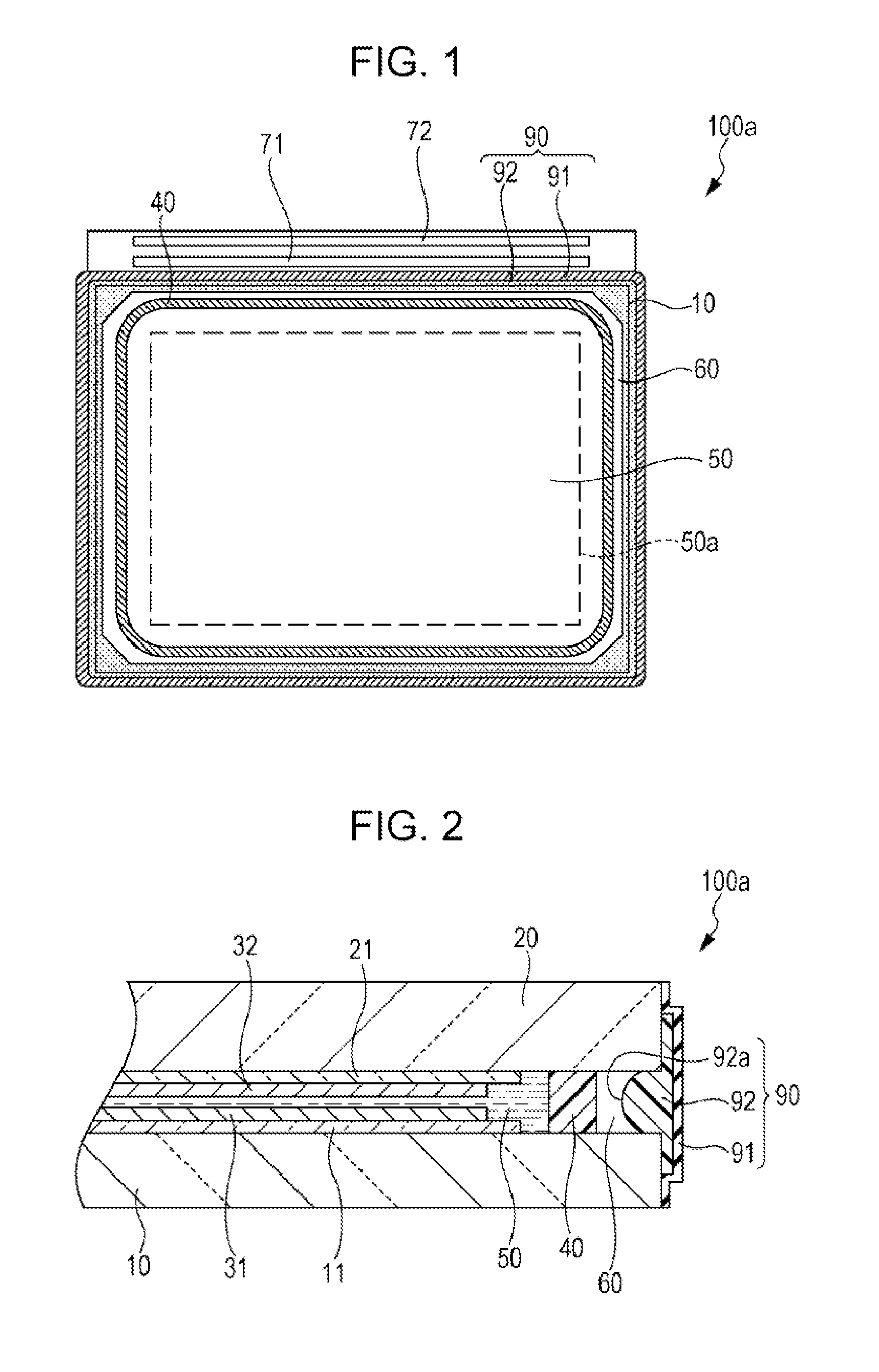
[0039]FIG. 1 is a schematic plan view illustrating a structure of a liquid crystal device as an example of electro-optical devices of the invention. FIG. 2 is a schematic sectional view illustrating part of the structure of the liquid crystal device as an example of electro-optical devices of the invention. Hereinbelow, the structure of a liquid crystal device 100a will be described with reference to FIGS. 1 and 2.

[0040]In this embodiment, the liquid crystal device 100a is one used in, for example, a light valve of a liquid crystal projector. For example, the liquid crystal device 100a is a TFT (thin film transistor) active matrix liquid crystal device having TFT elements as pixel switching elements.

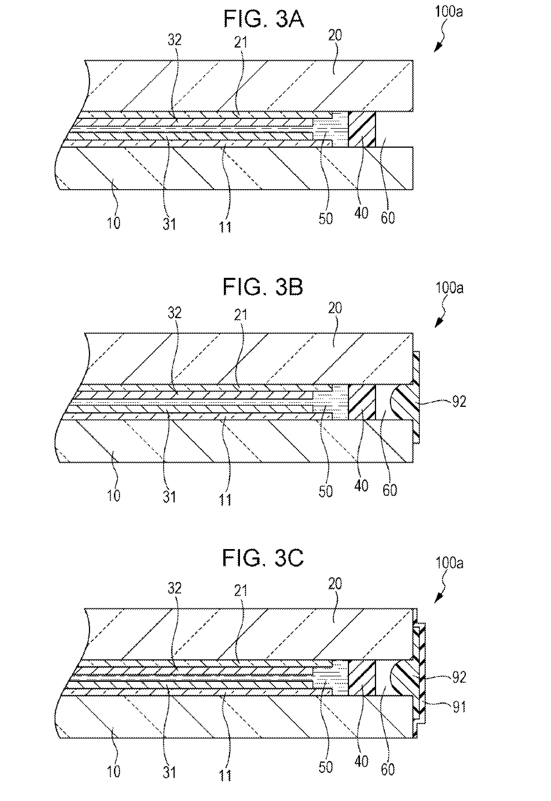
[0041]In the liquid crystal device 100a, an element substrate (a first substrate) 10 and a counter substrate (a second substrate) 20 are bonded to each other through a sealing material 40 that is in the form of substantially rectan...

second embodiment

B: Second Embodiment

[0068]The configuration of a liquid crystal device 100b according to the second embodiment is similar to that of the liquid crystal device 100a of the first embodiment described with reference to FIGS. 1 to 3C, except that while the gas barrier layer 90 in the liquid crystal device 100a of the first embodiment is formed with respect to the aligned lateral sides of the pair of substrates 10 and 20, a gas barrier layer 90a in the liquid crystal device 100b of the second embodiment is formed with respect to misaligned lateral sides of the substrates. FIG. 4 is a schematic plan view illustrating an example of the structure of the liquid crystal device according to the second embodiment of the invention. FIG. 5 is a schematic sectional view illustrating an example of the moistureproof layers in the liquid crystal device according to the second embodiment.

[0069]In the liquid crystal device 100b of this embodiment, as illustrated in FIG. 4, a counter substrate 20 and an...

third embodiment

C: Third Embodiment

[0073]Liquid crystal devices 100c and 100d according to the third embodiment are similar to the liquid crystal devices 100a and 100b of the first embodiment and the second embodiment, except that the liquid crystal devices 100c and 100d of the third embodiment contain filler particles 95 in the gas barrier layer. FIGS. 6A and 6B are schematic sectional views illustrating exemplary structures of the liquid crystal devices 100c and 100d according to the third embodiment.

[0074]In the liquid crystal devices 100c and 100d of this embodiment, as illustrated in FIGS. 6A and 6B, a gap material 43 such as glass fibers or glass beads is disposed to control the distance between the substrates to a prescribed value, for example, 1.5 μm to 3.5 μm. On the other hand, moistureproof resin layers 92 and 94 contain filler particles 95 having a smaller diameter than the gap material 43. Examples of the filler particles 95 include silica, alumina, mica and talc. The diameter of the f...


PUM


Abstract

A liquid crystal device includes an element substrate, a counter substrate, a liquid crystal disposed between the substrates, a sealing material disposed in the spacing between the element substrate and the counter substrate and sealing the liquid crystal, a gas barrier layer disposed outside of the sealing material to cover the outside of the spacing and having a portion located in the spacing, and an gap region defined in at least a portion of the space between the sealing material and the gas barrier layer.

Description

BACKGROUND[0001]1. Technical Field[0002]The present invention relates to electro-optical devices and electronic apparatuses including the electro-optical devices.[0003]2. Related Art[0004]In general, liquid crystal devices used as optical modulators mounted on such apparatuses as liquid crystal projectors, or used as direct-view display devices mounted on such apparatuses as mobile phones are basically composed of a pair of substrates having electrodes. Conductive films (such as pixel electrodes and counter electrodes) and, in the case of liquid crystal devices, alignment layers for controlling the initial alignment of liquid crystal molecules are formed on the respective inner sides of the pair of substrates. The pair of these substrates are coupled together through, for example, a sealing material, and thereby the substrates are bonded to each other. To constitute a liquid crystal device, a liquid crystal is sealed in the region enclosed by the sealing material.[0005]As devices su...

Claims


Application Information

Patent Timeline
IPC IPC(8): G02F1/1339
CPCG02F1/1339G02F1/0107G02F1/1341
Inventor TERAO, KOICHI
Owner SEIKO EPSON CORP
Why Eureka
Try Eureka