Method for epitaxial growth of high-quality and large-size monocrystalline diamond

A single crystal diamond, epitaxial growth technology, applied in the direction of single crystal growth, single crystal growth, crystal growth, etc., can solve the problem of diamond layer adhesion and so on

Active Publication Date: 2020-05-29
UNIV OF SCI & TECH BEIJING
View PDF5 Cites 14 Cited by
  • Summary
  • Abstract
  • Description
  • Claims
  • Application Information

AI Technical Summary

Problems solved by technology

However, the adhesion problem of the diamond layer caused by the large difference in thermal expansion coefficient is an important difficulty
However, due to the large lattice mismatch problem between the transition layer and iridium, the deposition growth and dislocation density control of the metal iridium layer have also become important problems in single crystal diamond epitaxy (Comprehensive Hard Materials, 3, 269-304, ( 2014))

Method used


Image

  • Method for epitaxial growth of high-quality and large-size monocrystalline diamond

Examples


Embodiment 1

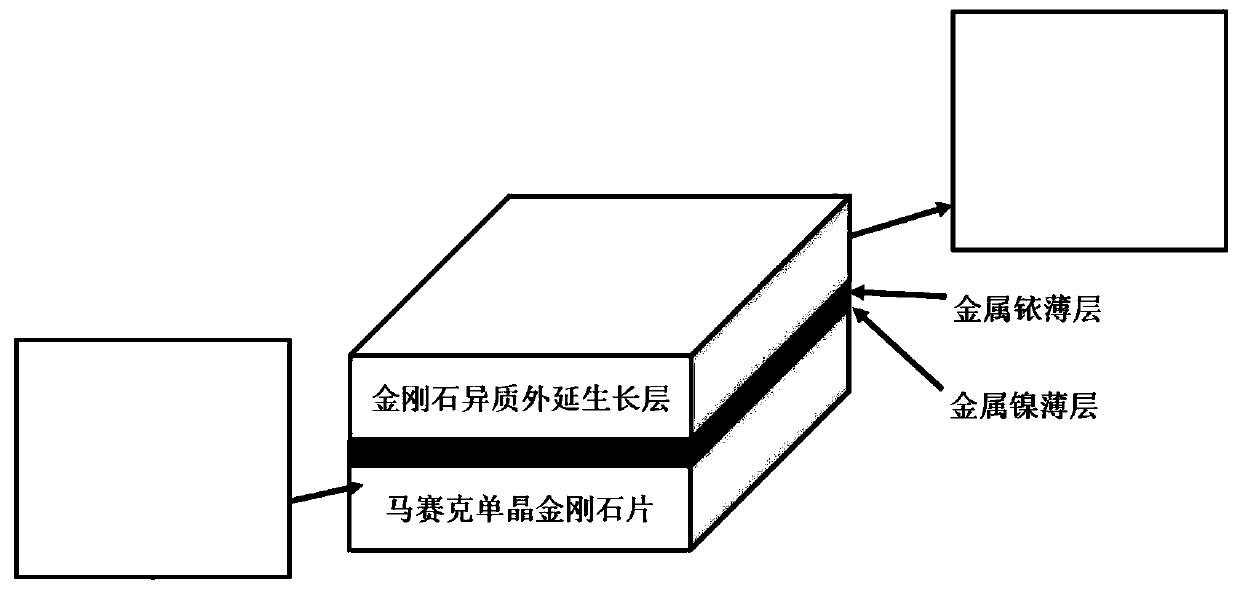
[0054] (1) Deposit a thin layer of metallic nickel by electron beam evaporation at a speed of 0.01nm / s under the condition of heating at 100°C on the ultra-flat mosaic single crystal diamond sheet after precision polishing and acid boiling cleaning pretreatment; (2) After the thickness of nickel thin layer deposition reaches 100nm, metal iridium is deposited at the same temperature, and metal iridium is deposited at a speed of 0.01nm / s to a thickness of 15nm at the initial stage of deposition; (3) after the initial stage of metal iridium deposition, increase the substrate heating Temperature to 700°C, continue to deposit metal iridium at a rate of 0.5nm / s to a thickness of 150nm; (4) Use a microwave plasma chemical vapor deposition system to control the input power to 1.5kW and the chamber pressure to 10kPa under the condition of pure hydrogen gas , the temperature is 700 ℃ to clean the surface of iridium for 10min, and then the methane with the flow rate of hydrogen is 10:100 ...

Embodiment 2

[0056] (1) Deposit a thin layer of metallic nickel by electron beam evaporation at a speed of 0.02nm / s under the condition of heating at 200°C on the ultra-flat mosaic single crystal diamond sheet after precision polishing and acid boiling cleaning pretreatment; (2) After the thickness of nickel thin layer deposition reaches 150nm, metal iridium is deposited at the same temperature, and metal iridium is deposited at a speed of 0.01nm / s to a thickness of 20nm in the initial stage of deposition; (3) after the initial stage of metal iridium deposition, increase the substrate heating Temperature to 800°C, continue to deposit metal iridium at a rate of 0.5nm / s to a thickness of 150nm; (4) Use a microwave plasma chemical vapor deposition system to control the input power to 1.5kW and the cavity pressure to 10kPa under the condition of pure hydrogen gas , the temperature is 700 ℃ to clean the surface of iridium for 20min, and then the methane with the hydrogen flow ratio of 12:100 is ...

Embodiment 3

[0058] (1) Deposit a thin layer of metallic nickel by electron beam evaporation at a speed of 0.03nm / s under the condition of heating at 300°C on the ultra-flat mosaic single crystal diamond sheet after precision polishing and acid boiling cleaning pretreatment; (2) After the thickness of nickel thin layer deposition reaches 150nm, metal iridium is deposited at the same temperature, and metal iridium is deposited at a speed of 0.01nm / s in the initial stage of deposition until the thickness reaches 30nm; (3) after the initial stage of metal iridium deposition, increase the substrate heating Temperature to 900°C, continue to deposit metal iridium at a rate of 0.5nm / s to a thickness of 200nm; (4) Use a microwave plasma chemical vapor deposition system to control the input power to 1.5kW and the cavity pressure to 10kPa under the condition of pure hydrogen gas , the temperature is 700 DEG C to clean the surface of iridium for 30min, and then feed methane with a flow ratio of 15:100...


PUM

PropertyMeasurementUnit
surface roughnessaaaaaaaaaa
particle sizeaaaaaaaaaa
diameteraaaaaaaaaa

Abstract

The invention discloses a method for epitaxial growth of high-quality and large-size monocrystal diamond, and belongs to the field of preparation of semiconductor materials. The method is characterized in that the surface roughness of a large-size single crystal diamond sheet grown through mosaic splicing is reduced to be lower than 0.2 nm through precision polishing; then electron beam evaporation is adopted to deposit metal nickel with the thickness of 100-200 nm on the surface of a substrate at the speed of 0.01-0.1 nm/s while the substrate is heated at the temperature of 100-500 DEG C, andthen metal iridium is deposited at the speed of 0.01-0.5 nm/s; after the thickness of iridium reaches 15-40 nm, the temperature of the heated substrate is increased to 700-1000 DEG C, meanwhile, thedeposition speed is increased to 0.5-1 nm/s, and finally, an iridium thin layer with the total thickness of 150-300 nm is deposited; then a plasma chemical vapor deposition technology is adopted to pre-deposit a 4-10 nm amorphous carbon layer after the iridium surface is cleaned by hydrogen plasma so as to promote the enrichment of carbon atoms on the sub-surface of the iridium thin layer; and finally, after the substrate is subjected to pure hydrogen plasma etching for 6-15 s, the negative bias voltage and the methane flux are regulated to achieve bias voltage in-situ nucleation of the large-size single crystal diamond on the iridium surface and subsequent non-bias voltage epitaxial growth.

Description

Technical field: [0001] The invention relates to the field of preparation of matrix materials for semiconductors. In particular, the preparation of high-quality large-size single crystal diamond provides a material preparation basis for the further realization of diamond-based semiconductor devices. That is, by depositing a metal nickel transition layer and a thin iridium layer on a high-gloss large-scale mosaic splicing single-crystal diamond self-supporting substrate. And the chemical vapor deposition method is used to pre-deposit an amorphous carbon thin layer on the surface of metal iridium, followed by pure hydrogen etching, and finally adjust the methane flux to realize the single-oriented crystallization of the iridium thin layer and the in-situ nucleation and growth of diamond, which is highly efficient. High-quality and large-size single crystal diamond can be obtained by heteroepitaxial method. [0002] technical background [0003] Diamond has extremely excellent...

Claims


Application Information

Patent Timeline
Patent Type & Authority Applications(China)
IPC IPC(8): C30B29/04C30B25/18
CPCC30B25/183C30B29/04
Inventor 李成明郑宇亭邵思武朱肖华刘金龙魏俊俊陈良贤
Owner UNIV OF SCI & TECH BEIJING
Why Eureka
Try Eureka