Ditch and hole structure and filling method thereof
A technology of holes and grooves, applied in semiconductor/solid-state device manufacturing, electrical components, circuits, etc., can solve problems such as increasing trench capacitance impedance and device failure
- Summary
- Abstract
- Description
- Claims
- Application Information
AI Technical Summary
Problems solved by technology
Method used
Image

Examples
Embodiment Construction
[0059] Figure 6A~6F It shows that in the first embodiment of the present invention, single crystal silicon whiskers are filled in the columnar trenches by a vapor-liquid-solid process.
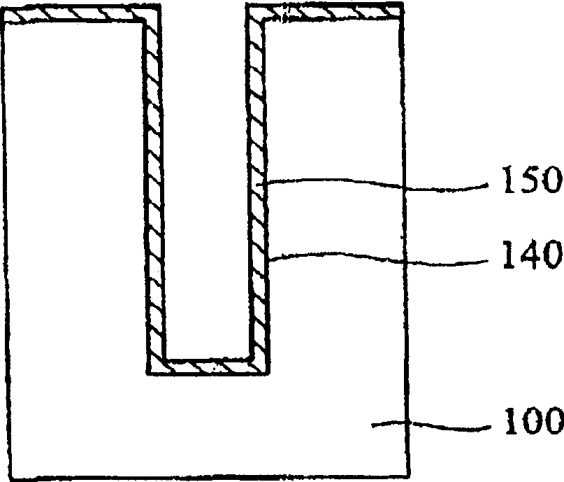
[0060] Please refer now Figure 6A , Showing that a part of the semiconductor substrate with empty trenches has been formed. The semiconductor substrate 600 is preferably composed of single crystal silicon. The trench 640 opens from the surface of the semiconductor substrate 600 and extends to the inside of the semiconductor substrate 600.
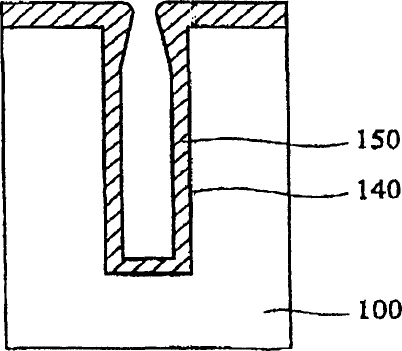
[0061] Please refer to Figure 6B , A silicon material layer 672 is, for example, chemical vapor deposition (chemical vapor deposition; CVD), silicon methane (SiH 4 ) Is a reactive gas and is formed on the surface of the trench 640. The silicon material layer 672 may contain only silicon, or may be silicon doped with, for example, arsenic.
[0062] Please refer to Figure 6C A metal layer 674 is formed on the surface of the silicon material layer 672 by, for...
PUM
 Abstract
Description
Claims
Application Information
 - R&D
- Intellectual Property
- Life Sciences
- Materials
- Tech Scout
- Unparalleled Data Quality
- Higher Quality Content
- 60% Fewer Hallucinations
Browse by: Latest US Patents, China's latest patents, Technical Efficacy Thesaurus, Application Domain, Technology Topic, Popular Technical Reports.
© 2025 PatSnap. All rights reserved.Legal|Privacy policy|Modern Slavery Act Transparency Statement|Sitemap|About US| Contact US: help@patsnap.com