Thin film for vacuum sucking wafer, wafer sucking device and vacuum sucking grinder

A vacuum adsorption and grinding head technology, applied in grinding equipment, grinding machine tools, transportation and packaging, etc., can solve problems such as wafer contamination, wafer damage, manufacturing process errors, etc., to improve wafer pass rate, improve time and human effect

Inactive Publication Date: 2005-12-28
UNITED MICROELECTRONICS CORP
View PDF0 Cites 2 Cited by
  • Summary
  • Abstract
  • Description
  • Claims
  • Application Information

AI Technical Summary

Problems solved by technology

[0008] However, the above-mentioned known technology of using vacuum suction to achieve wafer transfer has been found through actual operation that such a technology has a fatal flaw that is not easy to implement.
Because after the grinding process is over, when the internal pressure of the grinding head is to be restored to normal pressure to unload the wafer adsorbed on the film, due to the strong adsorption force between the film for vacuum adsorption wafer and the wafer, it often happens that the wafer cannot Normal unloading, that is to say, the wafer is still adsorbed on the film after the grinding head returns to normal pressure, which leads to failure in the manufacturing process and the possibility of wafer damage
[0009] In addition, if it is the current suction wafer device that transports and holds the wafer by vacuum, because there is no thin film between the porous plate used to absorb the wafer and the wafer to be adsorbed, there will be a vacuum at the same time of vacuum adsorption. Suction, attracting particles in the environment to the wafer, resulting in contamination of the wafer

Method used


Image

  • Thin film for vacuum sucking wafer, wafer sucking device and vacuum sucking grinder
  • Thin film for vacuum sucking wafer, wafer sucking device and vacuum sucking grinder
  • Thin film for vacuum sucking wafer, wafer sucking device and vacuum sucking grinder

Examples


Embodiment Construction

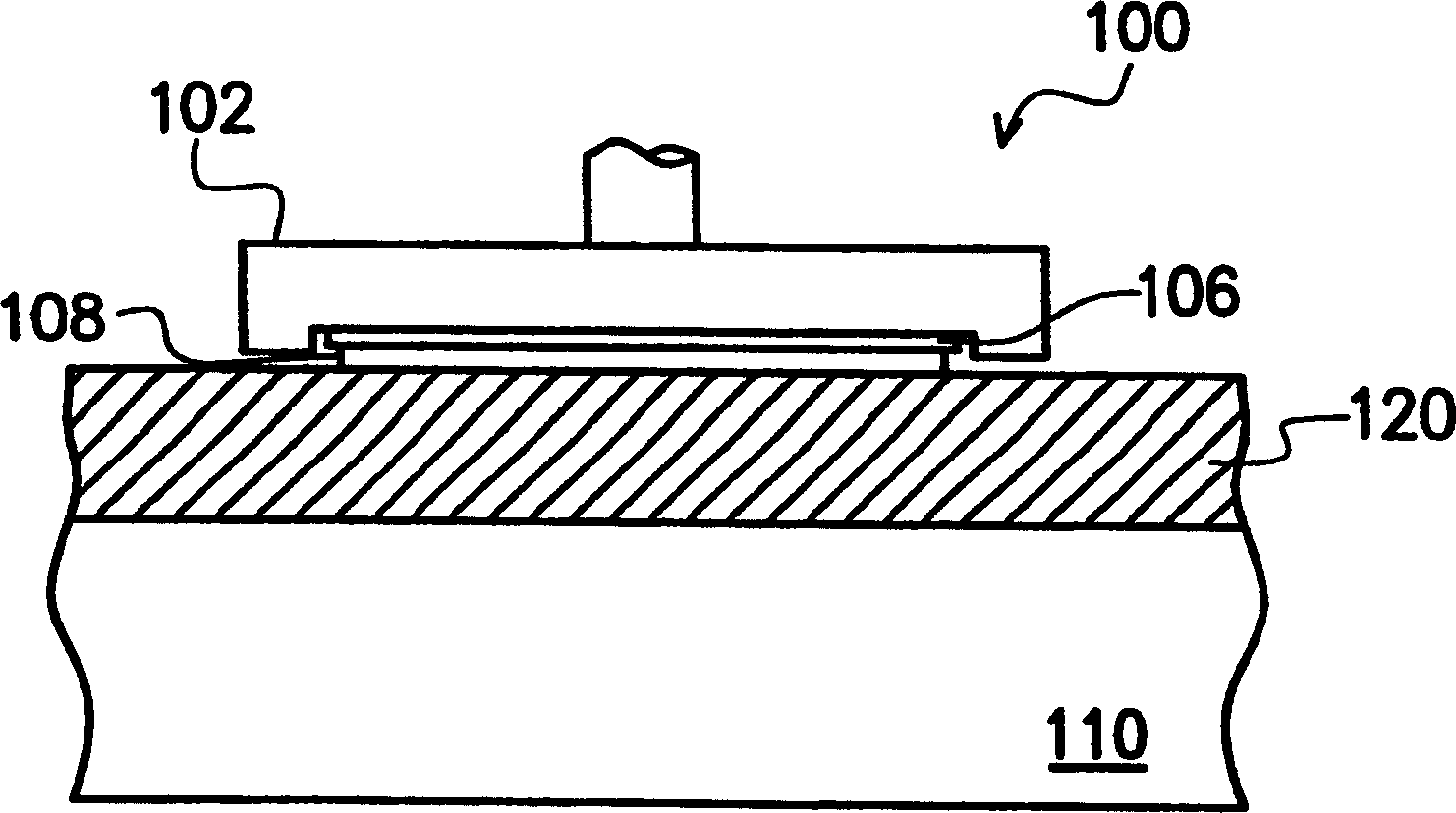
[0038] The membrane for vacuum adsorption wafer (Membrane) provided by the present invention can be applied in chemical mechanical polishing (Chemical Mechanical Polishing) device, as a membrane covering a porous plate in a vacuum adsorption polishing head (Polishing Head). However, the present invention can also be applied to other devices for vacuum suction (Suction), transfer (Transfer) and holding (Holding) wafers, and is not limited to this embodiment.

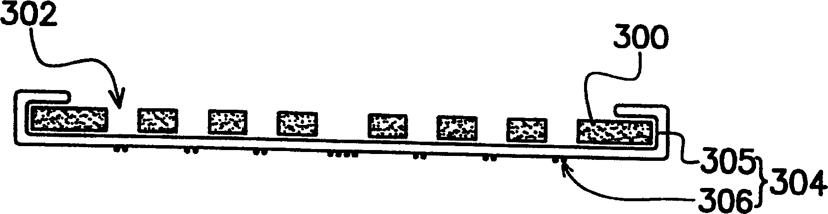
[0039] The chemical mechanical polishing device described in this embodiment generally includes a polishing head and a polishing table. Wherein, the grinding head is externally connected to a vacuum system, and also includes a chuck for fixing the wafer, and for the device in the chuck, please refer to the description of the preferred embodiment of the present invention. Figure 3A , Figure 3B and Figure 4 .

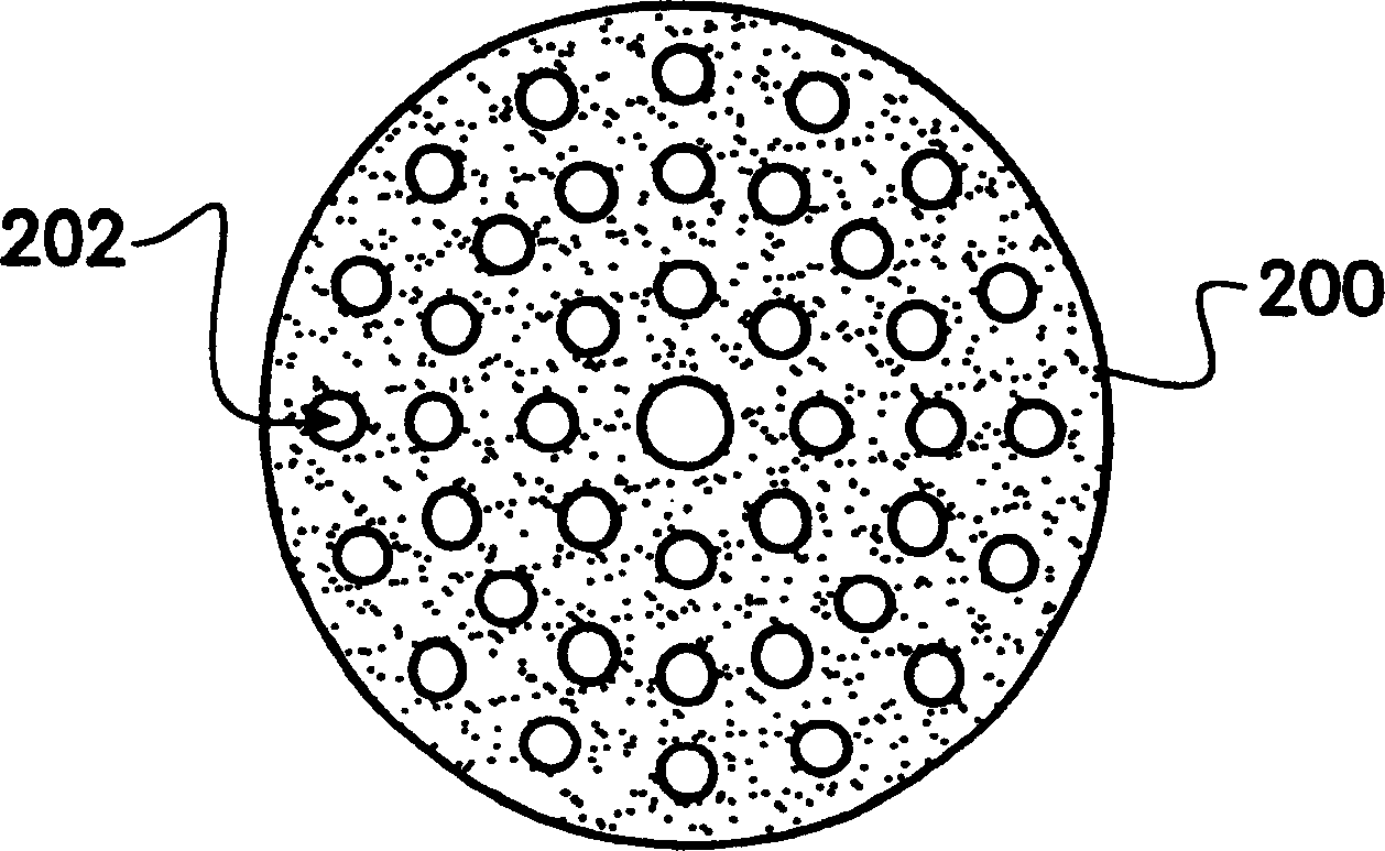
[0040] Figure 3A It is a schematic cross-sectional view of a porous plate for absorbing wafers and a film ...


PUM

PropertyMeasurementUnit
diameteraaaaaaaaaa
heightaaaaaaaaaa

Abstract

A film for vacuum adsorption to crystal wafer is suitable for the grinding head. Its apparatus has a main sheet body and several microparticles arranged at the positions on said main sheet body, where are corresponding to the holes on the adsorbing plate of grinding head. Said microparticles are used to adsorb wafer with lower adsorptive power and higher reliability.

Description

technical field [0001] The invention relates to a semiconductor transmission device, and in particular to a membrane (Membrane) for vacuum adsorption wafers. Background technique [0002] The mechanism used in the current wafer transfer system includes various methods, among which the method of using vacuum to absorb and hold wafers has been widely used. Taking the evolution of Chemical Mechanical Polishing devices as an example, please refer to figure 1 and figure 2 , and match the description below. [0003] figure 1 Shown is a partial schematic diagram of a known chemical mechanical polishing device. [0004] Please refer to figure 1 , the known chemical mechanical polishing device includes a polishing head (Polishing Head) 100 and a polishing platform (Polishing Table) 110, and a layer of polishing pad (Polishing Pad) 120 is covered on the polishing platform 110. Wherein, the grinding head 100 includes a chuck 102 for fixing the wafer 108, and there is also a laye...

Claims


Application Information

Patent Timeline
Patent Type & Authority Patents(China)
IPC IPC(8): B24B37/04B65G47/92B65G49/07G01N1/28H01J37/26H01L21/304
Inventor 陈慈信高明星林文钦纪华斌
Owner UNITED MICROELECTRONICS CORP
Why Eureka
Try Eureka