
Zero-delay slew-rate controlled output buffer

A technology of output buffer and signal output, which is applied to power oscillators, amplifiers with semiconductor devices/discharge tubes, amplifiers, etc., and can solve problems such as reduced switching speed, narrowed gap, and electromagnetic interference

Inactive Publication Date: 2000-02-02
ATMEL CORP
View PDF0 Cites 10 Cited by
  • Summary
  • Abstract
  • Description
  • Claims
  • Application Information

AI Technical Summary

Problems solved by technology

[0003] With conventional output buffers (i.e., inverter chains), the size of the output transistors is limited by the direct current (DC) operating characteristics
This leads to several problems: unacceptably high current peaks with simultaneous switching of many output buffers; inductive power supply noise causing large voltage drops; and electromagnetic interference due to high output edge switching rates. interference
[0005] The noise voltage generated is detrimental in many ways
First, non-switching circuits that share the same power and / or ground rail experience switching noise from active circuits, causing spurious transitions at the input of the non-switching circuit
Second, the switching speed is reduced due to noise narrowing the gap between the power supply potential and the ground voltage potential
Switching noise intensifies when switching of two or more circuits occurs simultaneously
[0006] Prior art solutions to these problems include reducing signal swing, but this comes at the expense of giving up TTL compatibility and having to provide additional supply voltages

Method used


Image

  • Zero-delay slew-rate controlled output buffer
  • Zero-delay slew-rate controlled output buffer
  • Zero-delay slew-rate controlled output buffer

Examples


Embodiment Construction

[0018] Best Mode for Carrying Out the Invention

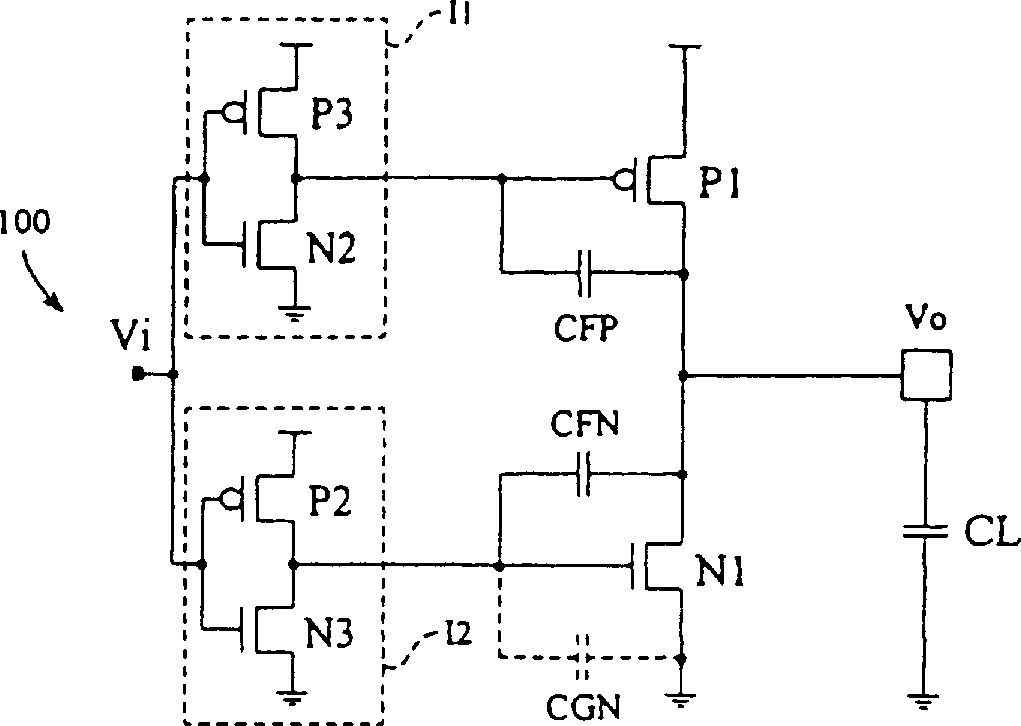
[0019] refer to figure 1 , the output buffer circuit 100 according to the present invention comprises an input node v for receiving a digital signal i . The input node is coupled to the control gates of four transistors: P-channel transistors P2 and P3, and N-channel transistors N2 and N3. Transistors P3 and N2 are coupled as inverter I1 and transistors P2 and N3 are coupled as inverter I2.

[0020] The output of buffer 100 is driven by transistors P1 and N1, whose drains are connected to the output node v o coupling. The source of transistor P1 is connected to V DD is coupled, while the source of transistor N1 is coupled to ground potential. The control gate of transistor P1 is coupled to the drains of transistors P3 and N2. Similarly, the control gate of transistor N1 is coupled to the drains of transistors P2 and N3.

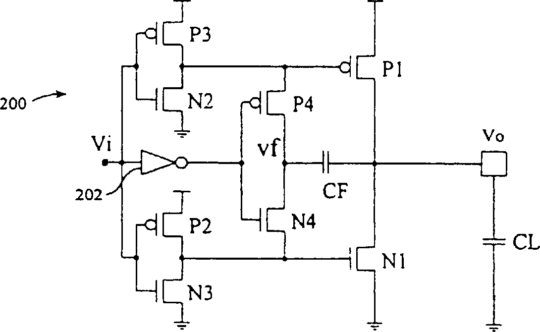
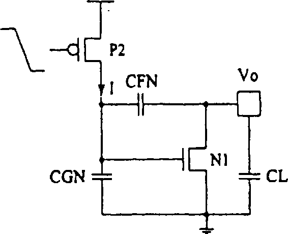
[0021] In addition, according to the present invention, from the output node v o The feedback path...


PUM


Abstract

An output buffer (100, 200) in accordance with the present invention exhibits a fixed output signal slew rate. The output signal behavior is independent of the capacitive load (CL) seen by the buffer. The circuit includes a capacitive feedback path from the output node to circuitry which drives the output transistors. In one embodiment, the feedback path comprises two capacitive elements (CFP, CFN), one which comes into play during a rising edge transition and the other which affects a falling edge transition. In a second embodiment, a single capacitive element (CF) is coupled to a switching circuit for use during either a falling transition or a rising transition. The second embodiment provides precharging of the output transistor gates, and so improves response time.

Description

technical field [0001] The present invention relates generally to output buffer circuits, and more particularly to a slew rate controlled output buffer circuit. Background technique [0002] The output buffer in the IC provides an interface to drive an external load, where the external load can be either capacitive or inductive. External capacitive loads typically consist of connecting lines, pins, conductors on a printed circuit board, and the input capacitance of the gate to which the output buffer is coupled. An inductive load typically consists of the power supply and the series parasitic inductance of the ground line providing the output buffer, which in turn couples to the external power supply and the ground rail on the printed circuit board. [0003] When using a conventional output buffer (ie, an inverter chain), the size of the output transistor is limited by the direct current (DC) operating characteristic. This leads to several problems: unacceptably high curre...

Claims


Application Information

Patent Timeline
IPC IPC(8): H03K5/12H03F3/30H03K17/16H03K19/003H03K19/0175
CPCH03K17/166H03F2200/45H03F3/3001H03F3/3022H03K19/00361H03K3/00
Inventor 弗洛朗·加西亚
Owner ATMEL CORP
Learn More