Level shift circuit
A level shift and circuit technology, applied in the direction of circuits, logic circuit connection/interface layout, electrical components, etc., can solve the problems of the deterioration of the action speed and slow action of the level shift circuit, and achieve the dispersion of suppressing the action delay and suppressing the lag. effect of effect
- Summary
- Abstract
- Description
- Claims
- Application Information
AI Technical Summary
Problems solved by technology
Method used
Image
Examples
no. 1 Embodiment
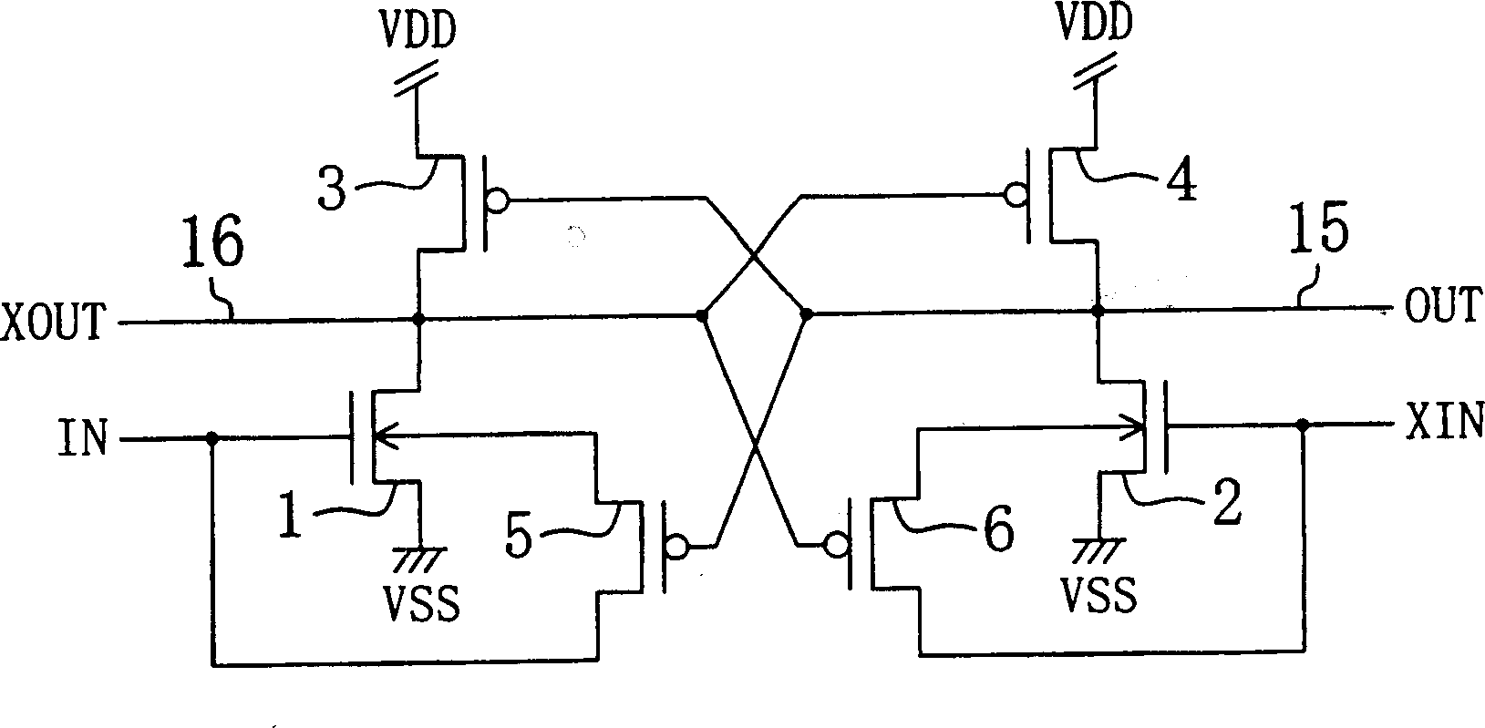
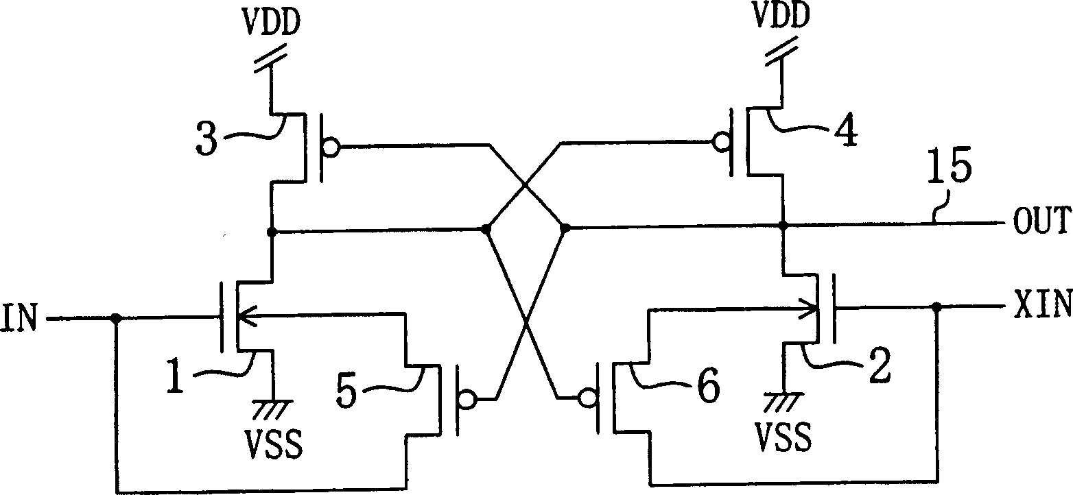
[0050] figure 1 A level shift circuit according to a first embodiment of the present invention is shown. In this figure, VDD is a high-voltage power supply, VSS is a ground power supply, IN is an input signal, XIN is an inverted input signal, OUT is an output signal, and XOUT is an inverted output signal.
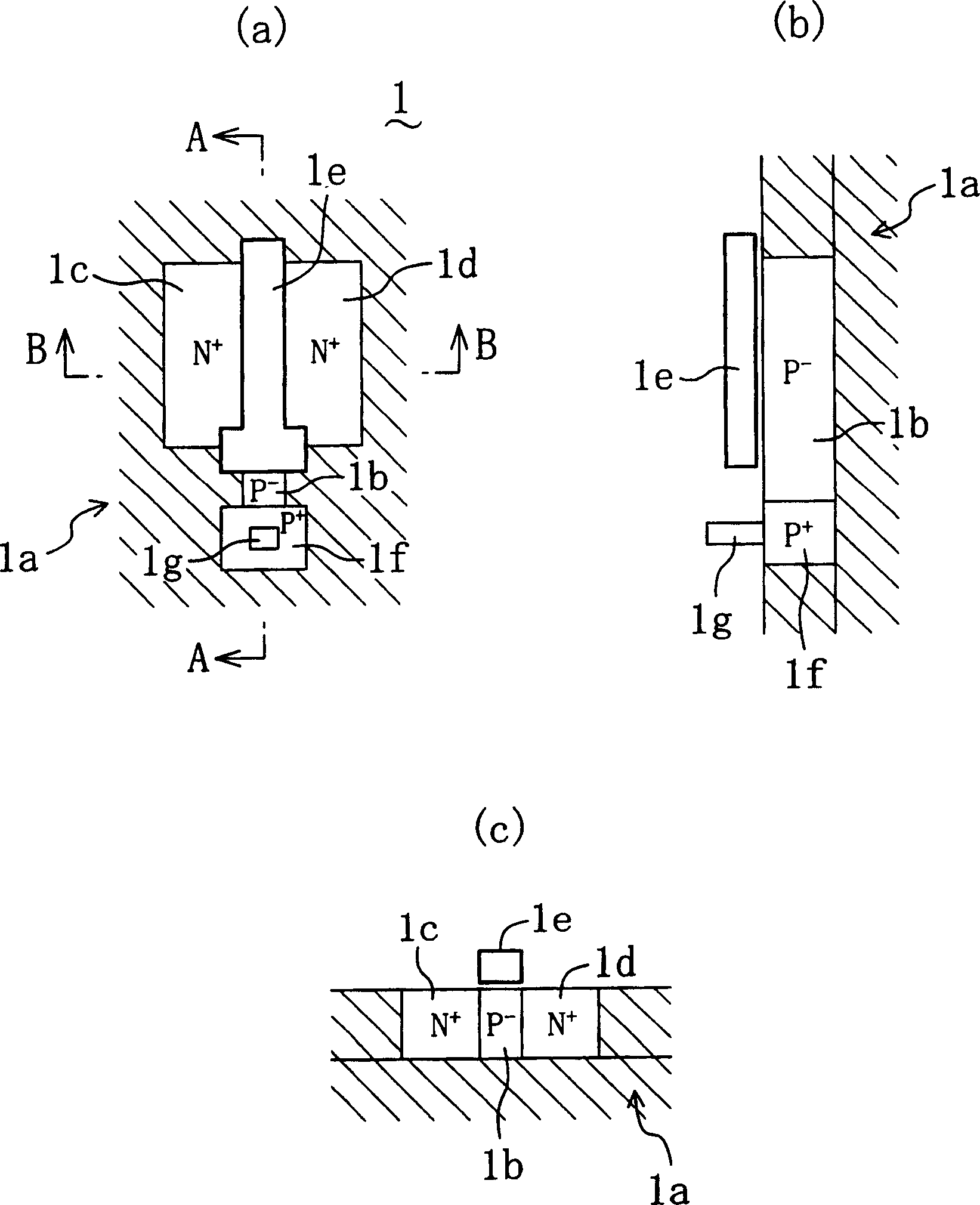
[0051] In addition, 1 is a first N-channel transistor for signal input to which the input signal IN is input to the gate, and 2 is a first N-channel transistor for signal input to which the inverted input signal XIN is input to the gate. 2N-channel transistors, the sources of the two transistors 1 and 2 are connected to the ground voltage VSS. 3 and 4 are the first and second P-channel transistors whose sources are connected to the high-voltage power supply VDD, and between these two P-channel transistors 3 and 4, a gate of a P-channel transistor is formed. pole is connected to the cross-coupling connection of the drain of another P-channel type transistor. The drain of...
no. 2 Embodiment
[0071] Figure 7 A level shift circuit according to a second embodiment of the present invention is shown.
[0072] The level shift circuit shown in this figure has the following features: First and second N-channel transistors 7 and 8 for resetting are added to the structure of the level shift circuit of the first embodiment described above. The source of the first N-channel transistor 7 used for reset is connected to the ground power supply (low power supply voltage) VSS, the drain is connected to the substrate of the first N-channel transistor 1 for signal input, and the The output signal OUT of the signal line 15 is input to the gate. Similarly, the source of the 2nd N-channel transistor 8 for reset is connected to the ground power supply (low power supply voltage) VSS, and the drain is connected to the substrate of the 2nd N-channel transistor 2 for signal input. , the inverted output signal XOUT of the signal line 16 is input to the gate.
[0073] In this embodiment, ...
no. 3 Embodiment
[0079] Figure 9 A level shift circuit according to a third embodiment of the present invention is shown. The level shifting circuit of this figure has the following features: In the above Figure 7 In the configuration of the level shift circuit of the second embodiment shown, first and second delay elements 9 and 10 are added. The first delay element 9 is arranged between the signal line 15 for outputting the signal OUT and the gate of the first N-channel transistor 7 for reset. The second delay element 10 is arranged between the signal line 16 of the inverted output signal XOUT and the gate of the second N-channel transistor 8 for reset.
[0080] The level shifting circuit of this embodiment has the structure of the level shifting circuit of the above-mentioned second embodiment, so as described above, only when the input signal IN and the inverted input signal XIN rise and change, these signals are received on the gate The N-channel transistors 1 and 2 have a substrate ...
PUM
 Abstract
Description
Claims
Application Information


