Method for driving power semiconductor element

A technology of power semiconductors and components, applied in the direction of semiconductor devices, output power conversion devices, electrical components, etc., can solve the unaccepted and complicated problems of double-door GTO

Inactive Publication Date: 2006-04-26
ABB (SCHWEIZ) AG
View PDF0 Cites 2 Cited by
  • Summary
  • Abstract
  • Description
  • Claims
  • Application Information

AI Technical Summary

Problems solved by technology

So the timing diagram for driving a two-door GTO is much more complicated than a typical GTO
For this reason, the two-door GTO was not accepted in practice, despite being known more than a decade ago and possibly having considerable merit

Method used


Image

  • Method for driving power semiconductor element
  • Method for driving power semiconductor element
  • Method for driving power semiconductor element

Examples


Embodiment Construction

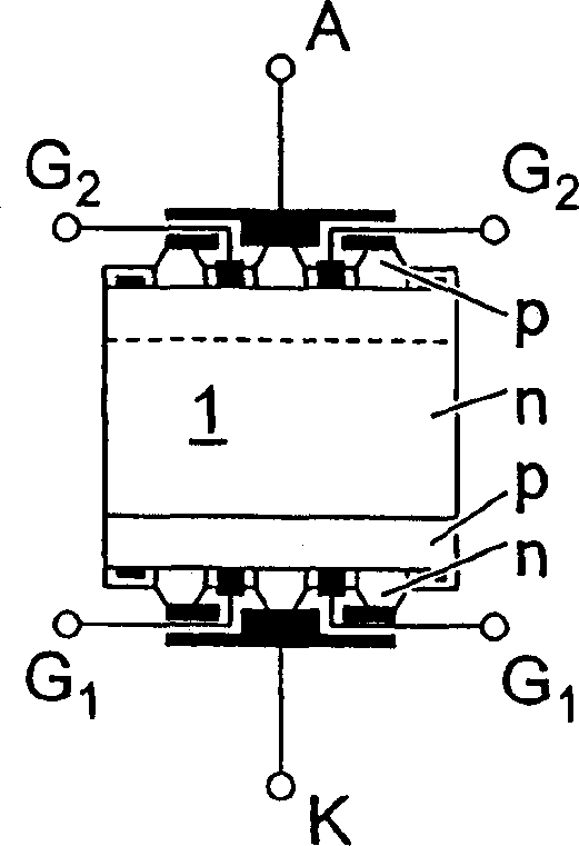
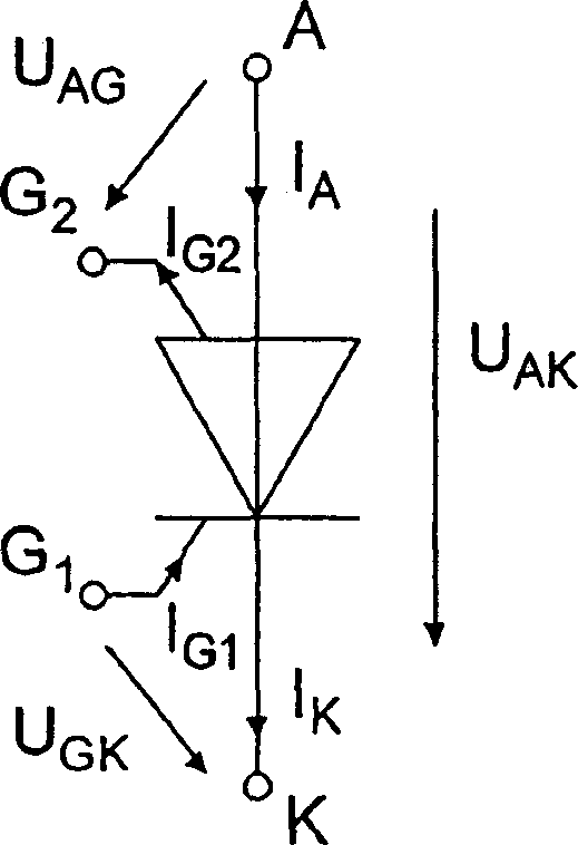
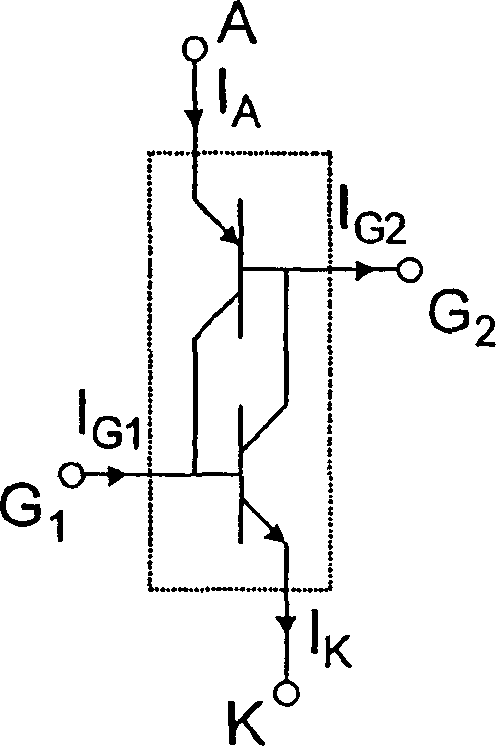
[0035] In all figures, the same reference signs correspond to the same working parts.

[0036] The integrated gate double transistor IGDT has a substrate with four semiconductor layers, on each side of which two electrical connections are provided.

[0037] figure 1 Diagrammatically showing the cross-section of this IGDT with four differently doped semiconductor layers,

[0038] - an anode layer with p-type doping outside the anode,

[0039] - a two-part n-type doped base layer with integrated n-type buffer,

[0040] - a p-type doped base layer, and also

[0041] - an n-type doped cathode layer outside the cathode.

[0042] There is a main connection terminal on both sides of the IGDT, anode A and cathode K, and a gate connection terminal, the first gate G 1 On the cathode side, the second gate G 2 on the anode side.

[0043] figure 2 The symbol of IGDT is shown. In this specification, positive values ​​according to the direction of the arrows in this diagram are use...


PUM


Abstract

The integrated gate double transistor (IGDT) has two controllable gates (G 1 , G 2 ), the first gate (G 1 ) is placed on the cathode side and is driven by the first gate current through the low inductance first gate connection, while the second gate (G 2 ) is placed on the anode side and driven by the second gate current through the low inductance second gate connection. During the IGDT cut-off operation, the rate of rise of the voltage on the IGDT is limited by the two gates. Limiting the rate of rise of the voltage across the IGDTs prevents voltage growth at different rates in the series-connected IGDT circuit and thus prevents overheating and destruction of individual IGDTs due to uneven loading.

Description

technical field [0001] The invention relates to the field of high-power electronics. [0002] The invention relates to a method of driving a power semiconductor element, which is an integrated gate double transistor (IGDT) with two controllable gates, the first gate being provided on the cathode side and connected by a low inductance The first gate connection is driven by the first gate current, and the second gate is provided on the anode side and driven by the second gate current through a low inductance second gate connection. [0003] The invention also relates to a circuit arrangement for implementing such a method. Background technique [0004] In the field of power semiconductor electronics, many kinds of fast and powerful semiconductor components have been created in order to find the best turn-off semiconductor components. In order to switch more power, it is necessary to reduce the losses of semiconductor components that are becoming smaller and smaller. Both dy...

Claims


Application Information

Patent Timeline
Patent Type & Authority Patents(China)
IPC IPC(8): H03K17/10H03K17/04H03K17/0812H01L29/744H01L29/74H02M1/08
CPCH03K17/0403H03K17/08124H03K17/105
Inventor O·阿佩尔多恩E·克洛尔P·斯特雷特A·韦伯
Owner ABB (SCHWEIZ) AG
Why Eureka
Try Eureka