
Method for making silicon nitride ROM

A technology of read-only memory and manufacturing method, which is applied in semiconductor/solid-state device manufacturing, electrical components, circuits, etc., and can solve the problems of complex ion implantation process, low reliability, breakdown, etc.

Inactive Publication Date: 2006-06-21
MACRONIX INT CO LTD
View PDF0 Cites 0 Cited by
  • Summary
  • Abstract
  • Description
  • Claims
  • Application Information

AI Technical Summary

Problems solved by technology

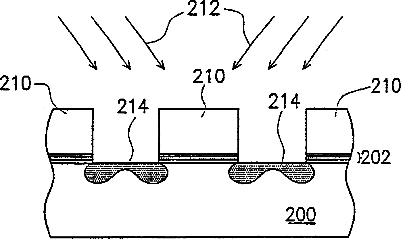
Therefore, when carrying out the pocket ion implantation process 212, it is necessary to use a large-angle implantation, so the ion implantation process is more complicated and the reliability is lower.
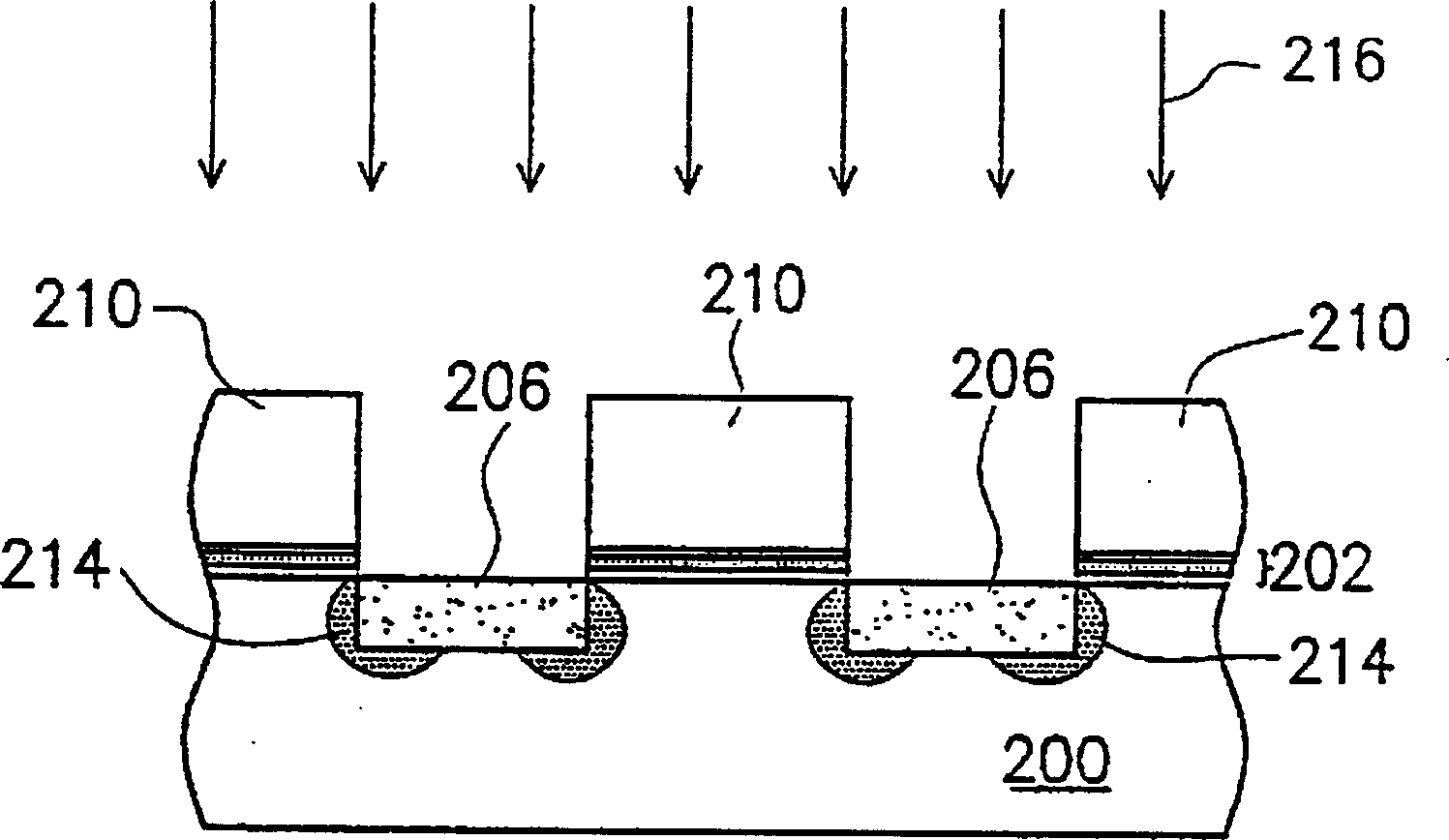
Moreover, the formed pocket-type doped region 214 cannot cover the contour of the buried bit line 206 well, so it is easy to cause the phenomenon of breakdown (Punch-Through)

Method used


Image

  • Method for making silicon nitride ROM
  • Method for making silicon nitride ROM
  • Method for making silicon nitride ROM

Examples


no. 2 example

[0046] In addition, the present invention can also be applied to a method for manufacturing a silicon nitride read-only memory (Nitride ReadOnly Memory, referred to as NROM), so as to prevent the dopant of the buried bit line from diffusing due to heat treatment, and to reduce the gap of the polysilicon pattern line width. In addition, the effective length of the channel can also be increased, so that the components can be miniaturized.

[0047] The front-end process of the silicon nitride read-only memory is as in the first embodiment Figure 3A to Figure 3C The same, and the mask pattern must be the gate pattern 324, the material of which is polysilicon, for example, and then refer to Figure 5 shown.

[0048] Figure 5 It is a cross-sectional view of the manufacturing process of a silicon nitride ROM according to the second embodiment of the present invention, and it is a process after forming the pocket-type doped region 318 .

[0049] Please refer to Figure 5 , usin...


PUM


Abstract

A method for manufacturing a silicon nitride read-only memory, comprising sequentially forming a first oxide layer, a capture layer, and a second oxide layer on a substrate, and then forming a mask pattern on the second oxide layer as an implant mask, and performing a Ion implantation process to form buried bit lines in the substrate. Then remove part of the mask pattern and the second oxide layer and capture layer not covered by the mask pattern, so as to increase the gap size of the mask pattern and expose part of the first oxide layer. Then, using the mask pattern as an implantation mask, a pocket ion implantation process is performed to form a pocket-type doped region around the contour of the buried bit line. Next, the mask pattern is removed, and the capture layer is used as a mask for heat treatment to form a buried bit line oxide layer on the substrate, and finally a word line is formed on the substrate.

Description

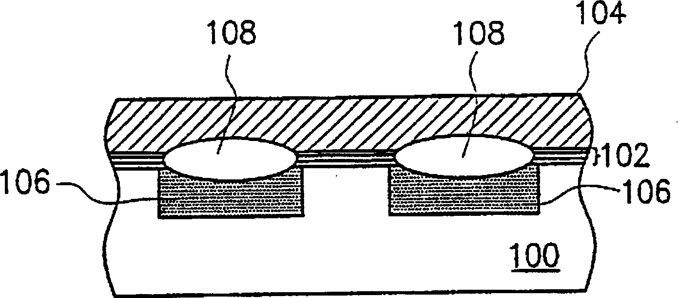
technical field [0001] The present invention relates to a method for manufacturing a semiconductor component, and in particular to a method for manufacturing a substrate / silicon oxide / silicon nitride / silicon oxide / silicon (Substrate / Oxide / Nitride / Oxide / Silicon, referred to as SONOS) component . Background technique [0002] figure 1 is a cross-sectional view of a known substrate / silicon oxide / silicon nitride / silicon oxide / silicon assembly. [0003] Please refer to figure 1 There is a layer of word lines 104 on the substrate 100, and between the substrate 100 and the word lines 104, there is a composite layer 102 composed of silicon oxide / silicon nitride / silicon oxide (Oxide / Nitride / Oxide, ONO for short) as a capture layer. (Trapping Layer) stacked (Stacked) structure, and the substrate 100 on both sides of the ONO layer 102 has a buried bit line 106, and a buried bit line oxide layer 108 is located on the buried bit line 106 Between the buried bit line 106 and the word l...

Claims


Application Information

Patent Timeline
Patent Type & Authority Patents(China)
IPC IPC(8): H01L21/8246H01L21/70H10B20/00
Inventor 叶彦宏范左鸿刘慕义詹光阳卢道政
Owner MACRONIX INT CO LTD
Learn More