Semiconductor device

A semiconductor and device technology, which is applied in the field of semiconductor devices to improve mechanical and electrical characteristics, can solve the problems of uneven current, the reduction of the maximum cut-off current of semiconductor chips, and the inability to cut off the current of MOS gate, so as to eliminate fluctuations and unevenness, improve The effect of the maximum cut-off current and the reduction in the number of screw fixations

Inactive Publication Date: 2006-09-20
KK TOSHIBA
View PDF0 Cites 0 Cited by
  • Summary
  • Abstract
  • Description
  • Claims
  • Application Information

AI Technical Summary

Problems solved by technology

If the magnification of the parasitic transistor increases, the parasitic thyristor composed of n source, P base, n base, and P emitter will easily become on state, and the current cannot be cut off by MOS gate.
In particular, if there is a part where the pressure is locally strong on the surface of the semiconductor chip, the parasitic thyristor is easily turned on in this part, and the current cannot be cut off by the MOS gate.
[0035] On the other hand, other parts use the MOS gate to cut off the current, so the current flowing into other parts is also concentrated on the part with high pressure, the operation of the thyristor expands, and the chip cannot be turned off from the on state, causing a self-locking (latch up) )Phenomenon
As a result, the problem is that the shutdown failure is caused, the maximum cut-off current is reduced, and the semiconductor chip is destroyed.
exist Figure 28 In the main circuit, the large current change rate di / dt in the main circuit generates a potential (electric power) in the gate circuit circuit, causing malfunction of the semiconductor chip and current concentration, gate voltage fluctuations, fluctuations in the main current Ic, etc.
In addition, the inductance of the gate circuit circuit is large, so it is also easily affected by the feedback from the collector current Ic to the gate, causing fluctuations in the gate voltage, etc., and even damage
[0039] Replacing the gate lead with a single-layer wiring sheet will also cause insufficient inductance drop, and the gate current Ig will flow to the emitter copper post 520 through which the main current Ic flows. Therefore, depending on the flow direction of the main current (current Time change of the vector) A potential is generated in the gate current path, a gate voltage different from the desired gate voltage of each chip is applied to the gate, current unevenness and current concentration occur, and the semiconductor chip is destroyed at a low current, etc. problem arises
[0040] As described above, the existing semiconductor devices for power control have problems of current concentration due to non-uniform surface pressure applied to the semiconductor chip, fluctuations in gate signal and collector current, etc., current concentration, etc., resulting in Causes the maximum cut-off current of the semiconductor chip to decrease and be damaged

Method used


Image

  • Semiconductor device
  • Semiconductor device
  • Semiconductor device

Examples


no. 1 Embodiment approach

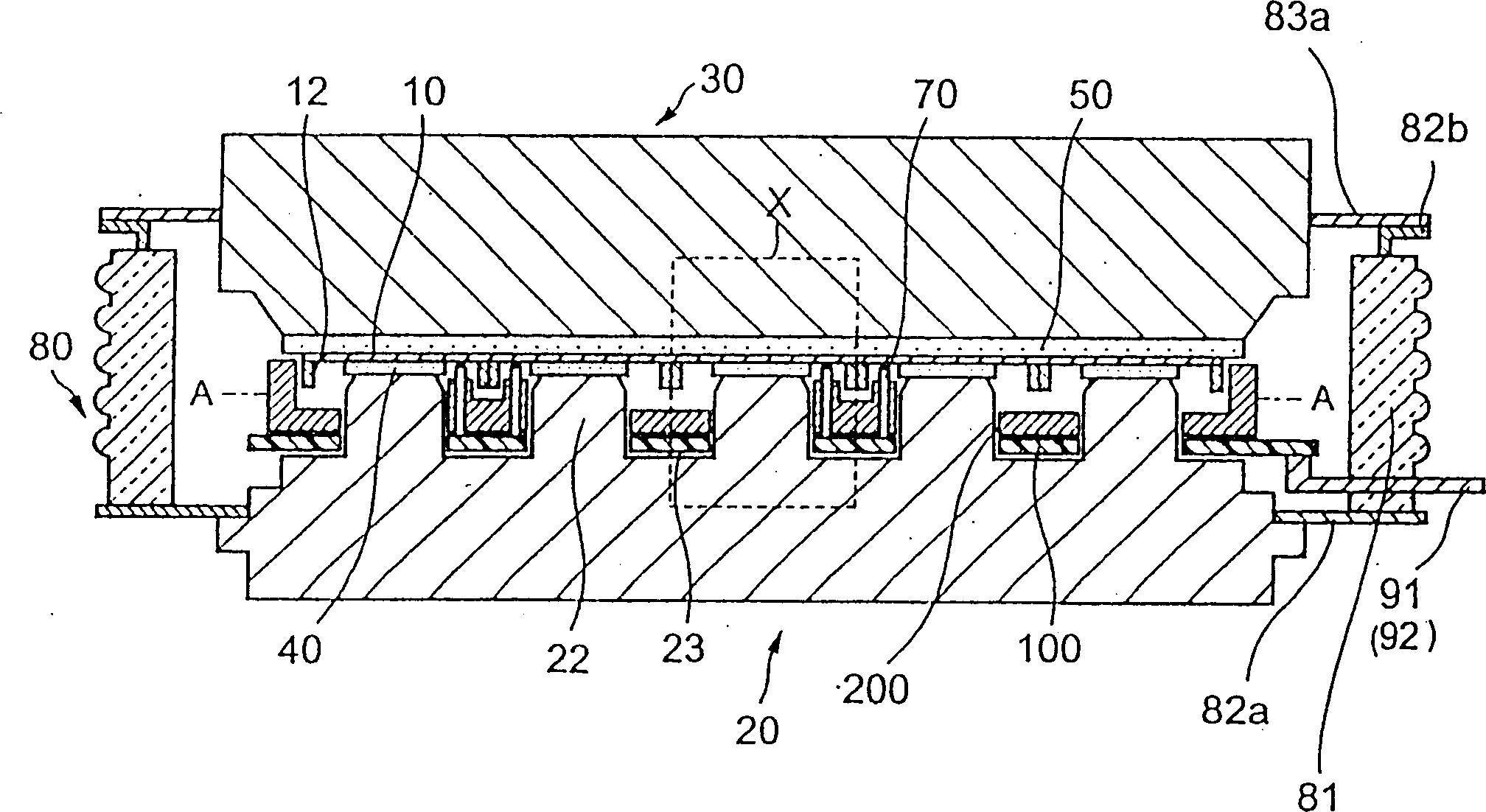
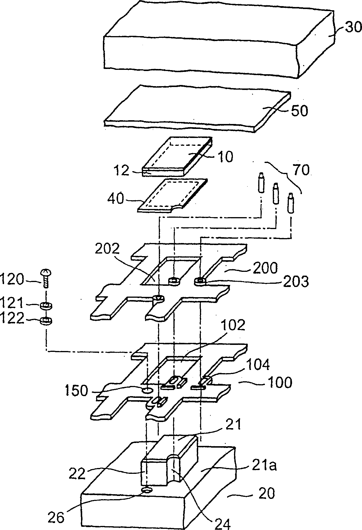
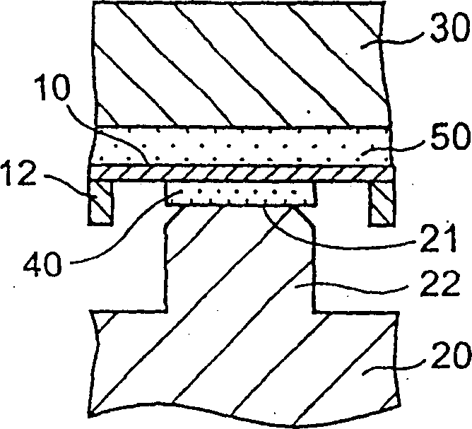
[0086] First, refer to figure 1 , Describes the outline of the configuration of the power control semiconductor device. figure 1 It is a cross-sectional view of a power control semiconductor device related to an embodiment of the present invention.

[0087] That is to say, semiconductor devices for power control, for example, a second main electrode member (hereinafter referred to as emitter copper pillar) 20 having a planar square pillar 22 and recessed portion 23 and a first main electrode member (hereinafter referred to as collector copper The pillars 30 are arranged in an opposed state. Semiconductor chips 10 such as IGBTs and IEGTs are arranged between the respective pillars 22 of the emitter copper pillar 20 and the aforementioned collector copper pillar 30 through molybdenum (Mo) buffer plates (hereinafter referred to as Mo buffer plates) 40 and 50, With the help of the above-mentioned emitter copper column 20 and the above-mentioned collector copper column 30 being press...

no. 2 Embodiment approach

[0162] Reference Figure 19 A detailed description will be given of the semiconductor device for power control according to the second embodiment of the present invention.

[0163] Figure 19 It is a schematic cross-sectional view showing the main part of the power control semiconductor device according to the second embodiment. In the figure, the same parts as those in the first embodiment are denoted by the same reference numerals, and repeated descriptions of the parts are omitted, and only the different parts are described.

[0164] In this embodiment and the above-mentioned first embodiment, regarding the contact between the emitter copper post 20 and the emitter wiring pattern 110 of the circuit wiring board 100, the circuit board mounting screw (second connecting conductor) 120 is used for connection in the above-mentioned first embodiment However, in this embodiment, the emitter pin (second connecting conductor) 300 is used for connection, and this point is different.

[...


PUM


Abstract

The present invention provides a semiconductor device which has a high maximum breaking current and hard to be broken. In the semiconductor device, a semiconductor chip 10 is pressue- welded to a part between a flat surface of a first main electrode member 30 and an upper surface 21a of a pillar 22 of a second main electrode member 20 via buffer plates 40, 50, and a gate electrode of the chip 10 is electrically connected with a gate signal wiring pattern of a circuit wiring board by using a gate connection conductor. One of a contact region between the pillar 22 of the second main electrode member 20 and the buffer plate 40 and a contact region between a part of the first main electrode member 30 facing the pillar 22 and the buffer plate 40 is formed small compared with a contact region between the buffer plate 40 on the second main electrode member 20 side and the semiconductor chip 10.

Description

Technical field [0001] The present invention relates to semiconductor devices such as semiconductor devices for power control, and more particularly to semiconductor devices whose mechanical and electrical characteristics can be improved by optimizing the packaging structure of the pressure-welding type device. Background technique [0002] It is known that general semiconductor devices for power control include IGBT (Insulated Gate Bipolar Transistor: Insulated Gate Bipolar Transistor) or IEGT (Injection Enhanced Gate Transistor: injection Enhanced gate transistor). [0003] Compared with the existing MOSFETs and bipolar transistors, these semiconductor devices for power control have the advantages of being able to withstand high voltages up to 6KV and at the same time using MOS gates for voltage driving. In addition, they are characterized by low power loss and are widely used. [0004] Hereinafter, with reference to the drawings, a conventional semiconductor device for power c...

Claims


Application Information

Patent Timeline
Patent Type & Authority Patents(China)
IPC IPC(8): H01L23/12H01L23/48H01L23/051
CPCH01L2924/14H01L2924/01005H01L2924/01039H01L2924/01015H01L2924/01006H01L2924/01078H01L2924/01047H01L2924/01029H01L2924/30107H01L2924/01013H01L23/051H01L2924/01074H01L2924/01082H01L2924/19042H01L2924/0101H01L2924/19043H01L2924/01004H01L2924/01023H01L2924/01042H01L2924/01079H01L2924/13034H01L2924/19041H01L2924/13091H01L2924/1305H01L2924/01033H01L2924/1301H01L2924/01002H01L2924/13055H01L24/72H01L25/072H01L2924/00
Inventor 大村一郎土门知一三宅英太郎
Owner KK TOSHIBA
Why Eureka
Try Eureka