
Semiconductor device with fuse

A semiconductor and fuse technology, which is applied in the fields of semiconductor devices, semiconductor/solid-state device manufacturing, semiconductor/solid-state device components, etc., and can solve the problems of substrate damage and reduction of fuse breakage processing margins.

Inactive Publication Date: 2006-12-13
SOCIONEXT INC
View PDF0 Cites 3 Cited by
  • Summary
  • Abstract
  • Description
  • Claims
  • Application Information

AI Technical Summary

Problems solved by technology

Since the dummy structure pattern is provided in the fuse circuit, the margin for the fuse breaking process may be lowered, or the substrate may be destroyed

Method used


Image

  • Semiconductor device with fuse
  • Semiconductor device with fuse
  • Semiconductor device with fuse

Examples


Embodiment Construction

[0032] First, new facts discovered by the present inventors during development will be described. First, an example of a process for forming a dummy structure region will be described.

[0033] like Figure 9A As shown, on the surface of a silicon substrate 1, a silicon oxide film 2 having a thickness of about 10 nm is grown by oxidation with hydrochloric acid at 900°C. On this silicon oxide film 2, a silicon nitride film 3 is grown to a thickness of about 110 nm by chemical vapor deposition (CVD).

[0034] A photoresist pattern is formed on silicon nitride film 3, and silicon nitride film 3 and silicon oxide film 2 are etched by anisotropic etching. The photoresist pattern is then removed. By using silicon nitride film 3 as a mask, silicon substrate 1 is anisotropically etched. For example, an approximately 300 nm thick surface layer of the silicon substrate is etched away to form trenches approximately 300 nm deep.

[0035] like Figure 9B As shown, a silicon oxide fil...


PUM


Abstract

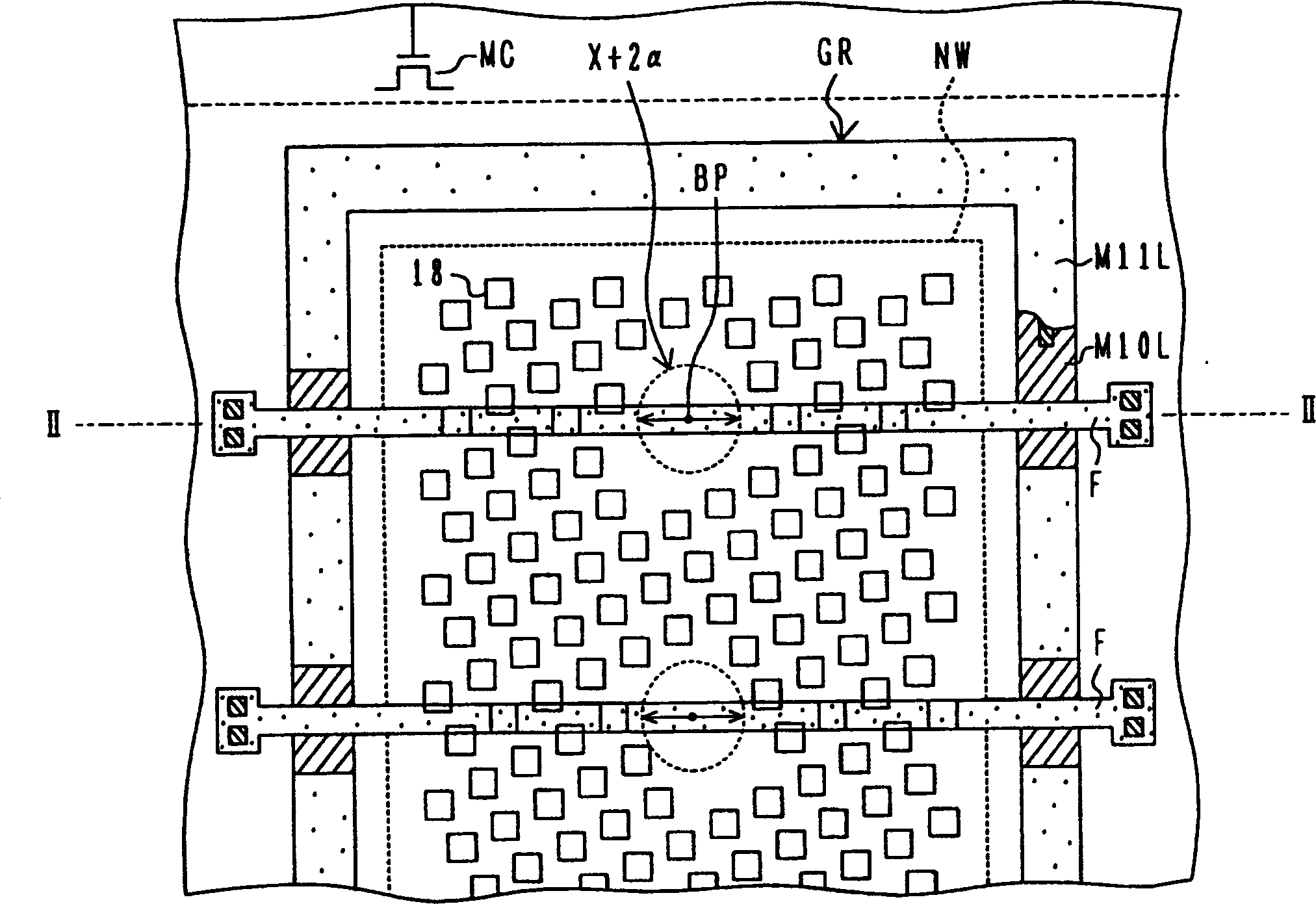
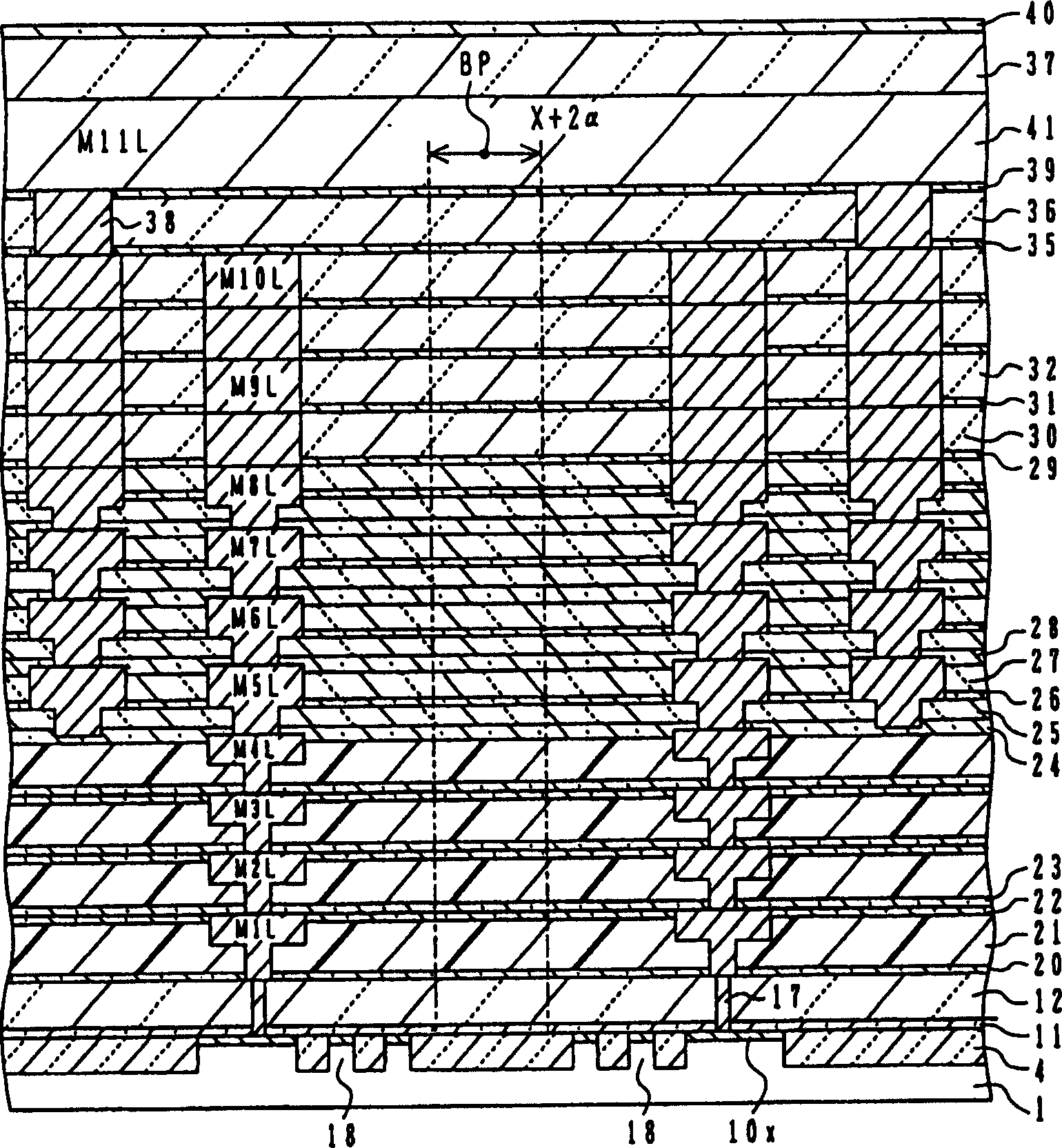
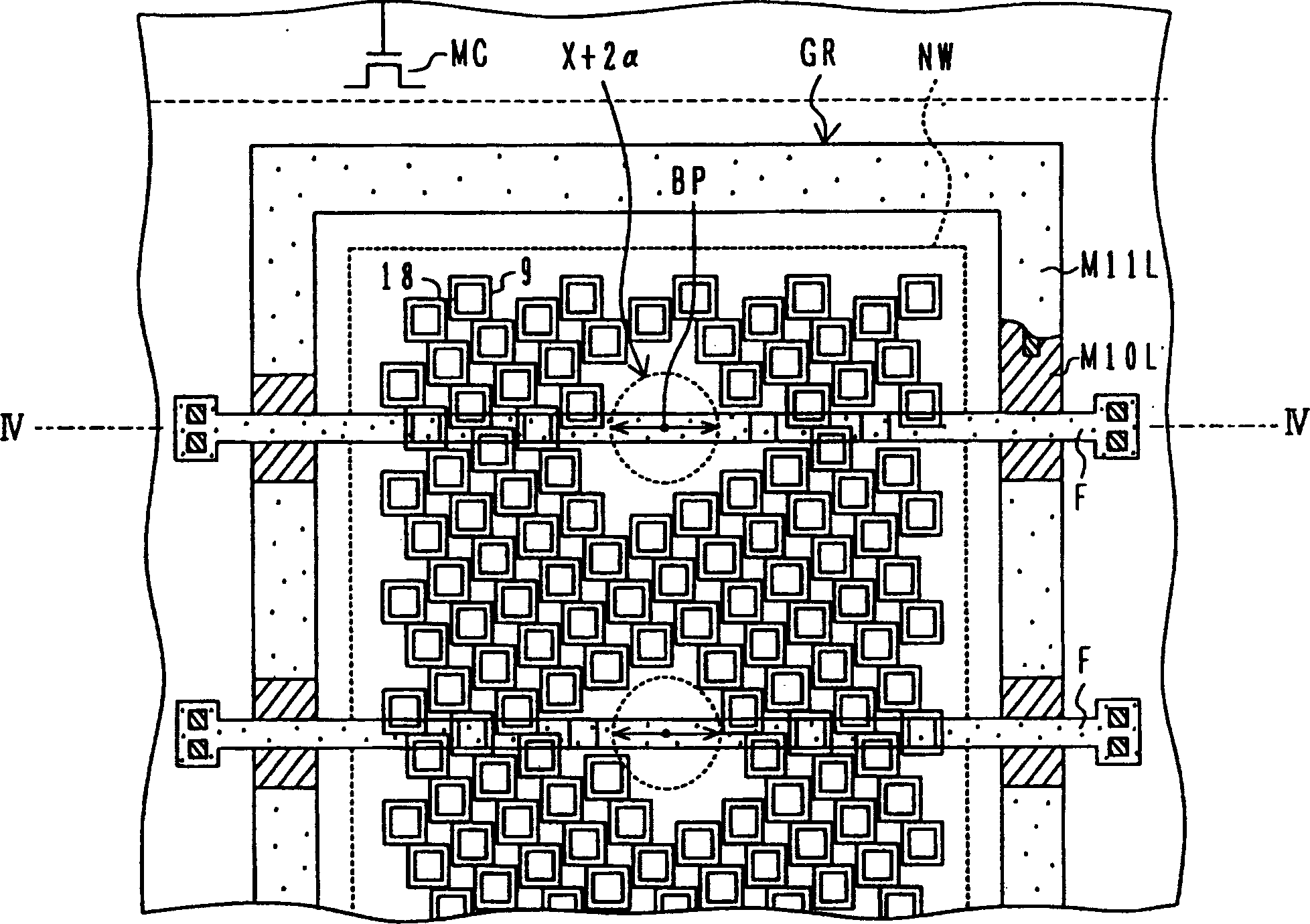
A semiconductor device has: a semiconductor substrate having a principal surface; a fuse circuit formed above the principal surface, the fuse circuit having fuse elements each having a predetermined breaking point; a first trench isolation region formed in a surface layer of the semiconductor substrate under the fuse circuit; and a plurality of active region dummies formed through the first trench isolation region in an area excepting a predetermined area around the predetermined breaking point. Although a dummy structure is formed also in a fuse circuit, a breaking margin is prevented from being lowered and a substrate damage is avoided, while surface flatness and line width controllability are ensured.

Description

technical field [0001] The present invention relates to a semiconductor device, and more particularly, the present invention relates to a semiconductor device having a fuse circuit and a dummy structure which does not function as an electronic circuit. The dummy structure may be a dummy active region, a dummy gate electrode, and the like. Background technique [0002] Recently, the integration level of semiconductor integrated circuit devices is very high, so shallow trench isolation (STI), which is beneficial to planarization, has been adopted instead of local oxidation of silicon (LOCOS) as an isolation technology. Since the gate length has become shorter than in the past, high patterning accuracy is required to form the gate electrode. [0003] For example, a buffer silicon oxide film and a silicon nitride film are formed on a silicon substrate, and an opening penetrating through the buffer silicon oxide film and the silicon nitride film is formed, the opening having a s...

Claims


Application Information

Patent Timeline
Patent Type & Authority Patents(China)
IPC IPC(8): H01L23/525H01L27/06H01L21/3205H01L21/762H01L21/82H01L21/822H01L23/52H01L23/58H01L27/04
CPCH01L23/585H01L2924/0002H01L23/5258H01L21/76224H01L2924/00H01L21/82
Inventor 南条亮太大塚敏志泽田丰治助川和雄
Owner SOCIONEXT INC
Learn More