
Integrated circuit chips visual aligning method

A visual alignment, integrated circuit technology, applied in circuits, electrical components, electrical solid devices, etc., can solve the problems of neglecting the positioning error of the chip and the lead frame, limiting the calculation speed, reducing the alignment accuracy, etc., to ensure accuracy, The effect of improving accuracy and reducing measurement errors

Inactive Publication Date: 2007-02-14
HUAZHONG UNIV OF SCI & TECH
View PDF3 Cites 0 Cited by
  • Summary
  • Abstract
  • Description
  • Claims
  • Application Information

AI Technical Summary

Problems solved by technology

[0011] As a theoretical analysis, the above algorithm proposes some useful alignment algorithms, but it is not closely integrated with the specific production process, and the positioning error between the chip and the lead frame brought about by the SMT process is ignored.
At the same time, the above algorithm only applies to a single alignment mark. If a single mark has a large local deformation or measurement error, it is still used as an alignment mark, which will significantly reduce the alignment accuracy.
The entire alignment process includes the removal of defective chips such as ink dot marks, edge chipping scratches, and empty chips. The previous algorithm mainly uses a serial calculation process, and the calculation speed is limited.

Method used


Image

  • Integrated circuit chips visual aligning method
  • Integrated circuit chips visual aligning method
  • Integrated circuit chips visual aligning method

Examples


Embodiment Construction

[0047] The present invention will be further described below in conjunction with the accompanying drawings.

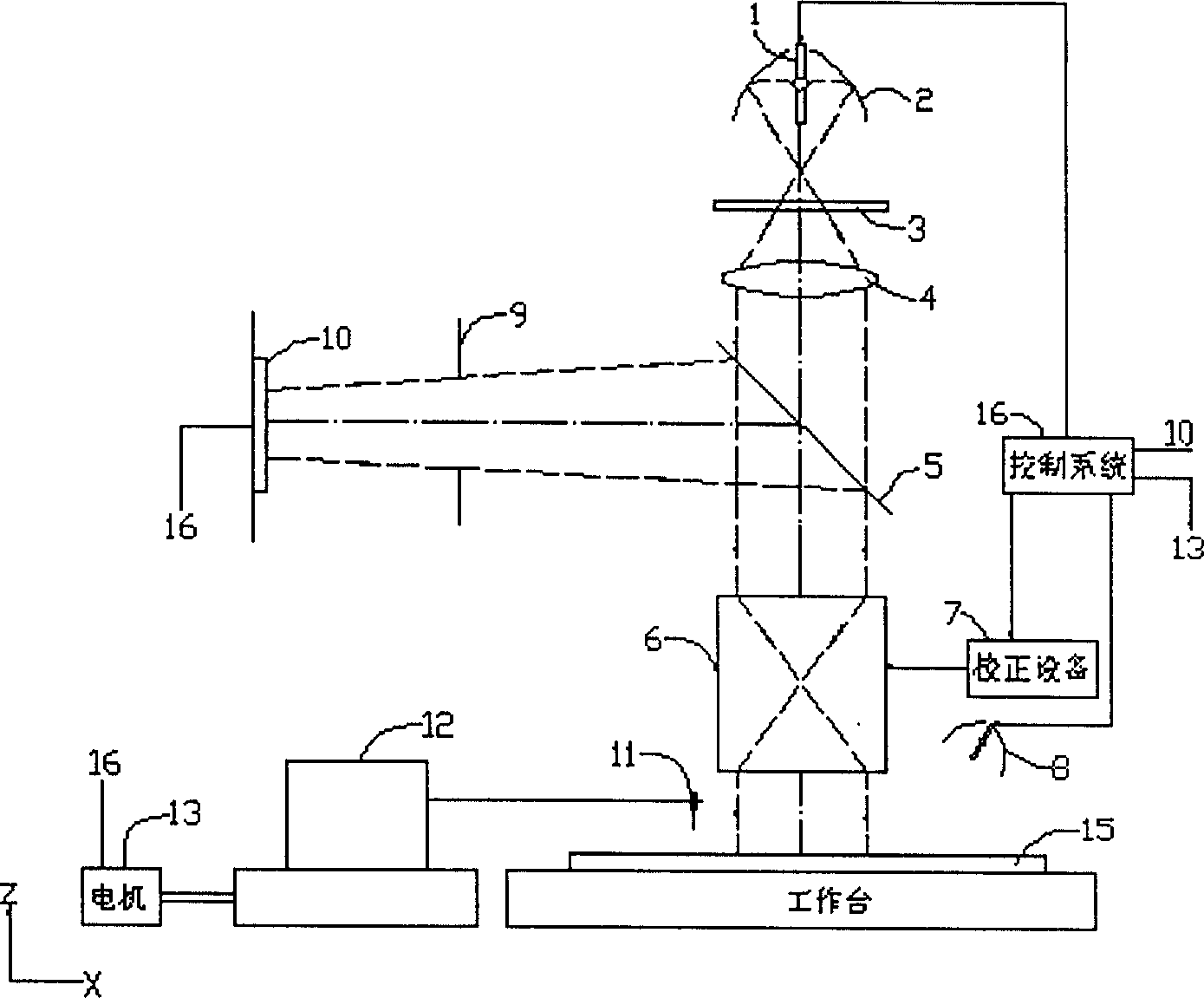
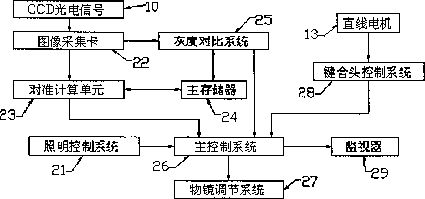
[0048] figure 2 An image vision system applied to the alignment method of the present invention is shown. After the light emitted from the coaxial lamp 1 is reflected by the elliptical mirror 2, the red light passes through the filter 3. Then the light passes through the homogenizing sheet 4 to form a parallel light beam perpendicular to the optical axis, passes through the beam splitter 5, and vertically irradiates the surface of the chip on the workbench 15. This light path is a coaxial light path. It produces the best contrast for flat, uniform graphics. In addition to the coaxial light 1, four side lights 8 composed of red light-emitting diode groups are fixed above the workbench 15. They are installed around the coaxial light and illuminate the chip at a certain angle. The side light 8 Produces the best contrast on surface unevenness and edges. In order to fu...


PUM


Abstract

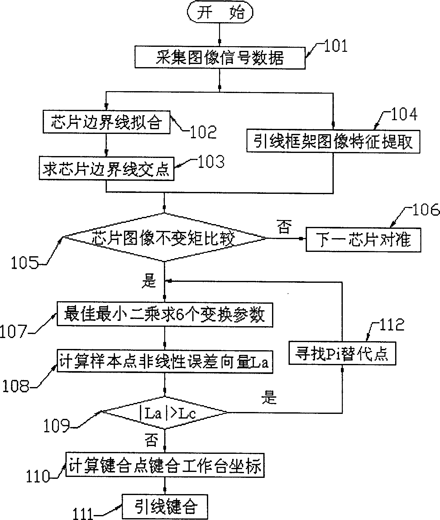
It is an integration circuit chip vision aligning method belonging to integration circuit chip seal method, which comprises the following steps: to select sample from the lead wire frame and chip; to get the sample measurement coordinates by image process and to measure the defect chip by image constant moment; to get the chip position transformation parameters to get the coordinates; to get the sample non-linear error by minus measurement coordinates from computation coordinates till the error is within the permitted value; finally to transform the bonding arranged coordinates into bonding workbench displacement coordinates.

Description

technical field [0001] The invention belongs to the packaging method of integrated circuit chips, and specifically relates to the visual alignment method of chips, which is suitable for chip bonding devices, calibration devices, and detection devices, and will be widely used in modern manufacturing industries such as semiconductor equipment, liquid crystal displays, and thin-film magnetic heads. use. Background technique [0002] In the IC and HIC manufacturing industry, the internal interconnection and lead-out wire connection processes of chips mainly include thermocompression welding, silicon-aluminum wire ultrasonic bonding, gold wire ball bonding, flip-chip bonding, and carrier tape bonding. Among them, the gold wire ball bonding process, as one of the main bonding processes, is widely used in the internal leads and lead-out interconnection processes of large-scale integrated circuits and large-scale thick-film hybrid integrated circuits; In the circuit, it is more wid...

Claims


Application Information

Patent Timeline
Patent Type & Authority Patents(China)
IPC IPC(8): H01L21/60G06F17/50
CPCH01L2224/80
Inventor 李小平聂宏飞李朝晖杨文建
Owner HUAZHONG UNIV OF SCI & TECH
Learn More