

Integrated circuit chips visual aligning method
A visual alignment, integrated circuit technology, applied in circuits, electrical components, electrical solid devices, etc., can solve the problems of neglecting the positioning error of the chip and the lead frame, limit the calculation speed, reduce the alignment accuracy, etc., to ensure the accuracy, The effect of improving accuracy and reducing measurement errors
- Summary
- Abstract
- Description
- Claims
- Application Information
AI Technical Summary
Problems solved by technology
Method used
Image

Examples
Embodiment Construction
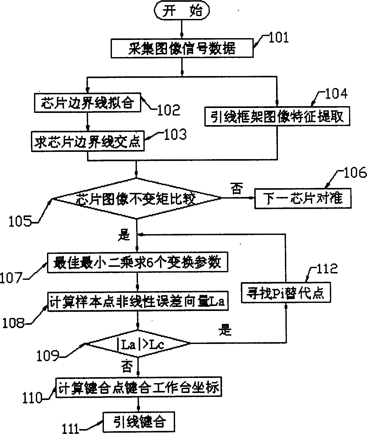
[0047] The present invention will be further described below in conjunction with the accompanying drawings.
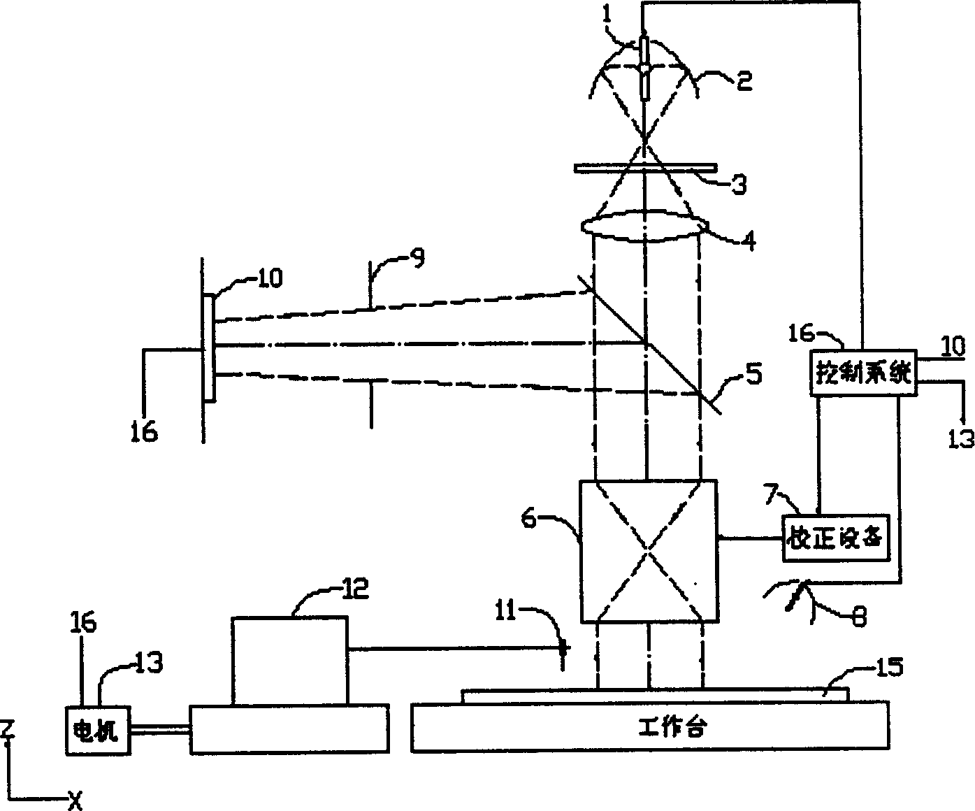
[0048] figure 2 An image vision system applied to the alignment method of the present invention is shown. After the light emitted from the coaxial lamp 1 is reflected by the elliptical mirror 2, the red light passes through the filter 3. Then the light passes through the homogenizing sheet 4 to form a parallel light beam perpendicular to the optical axis, passes through the beam splitter 5, and vertically irradiates the surface of the chip on the workbench 15. This light path is a coaxial light path. It produces the best contrast for flat, uniform graphics. In addition to the coaxial light 1, four side lights 8 composed of red light-emitting diode groups are fixed above the workbench 15. They are installed around the coaxial light and illuminate the chip at a certain angle. The side light 8 Produces the best contrast on surface unevenness and edges. In order to fu...
PUM
 Abstract
Description
Claims
Application Information