Manufacture of flash memory

A manufacturing method and memory technology, applied in semiconductor/solid-state device manufacturing, electrical components, circuits, etc., can solve the problems of increasing flash memory, poor reliability, and backwardness

Inactive Publication Date: 2002-01-23
VANGUARD INTERNATIONAL SEMICONDUCTOR CORPORATION
View PDF1 Cites 13 Cited by
  • Summary
  • Abstract
  • Description
  • Claims
  • Application Information

AI Technical Summary

Problems solved by technology

[0004] Obviously, the stacked gate flash memory manufactured by traditional technology has complicated process steps, resulting in poor reliability and lower yield, increasing manufacturing cost and affecting its competitiveness
Moreover, traditional technology will seriously affect its competitiveness when the integrated circuit manufacturing

Method used


Image

  • Manufacture of flash memory
  • Manufacture of flash memory
  • Manufacture of flash memory

Examples


Embodiment Construction

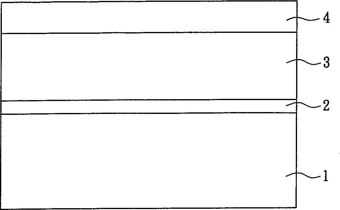
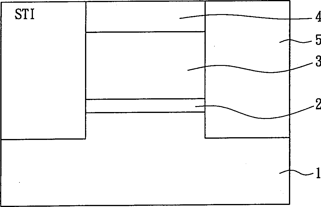
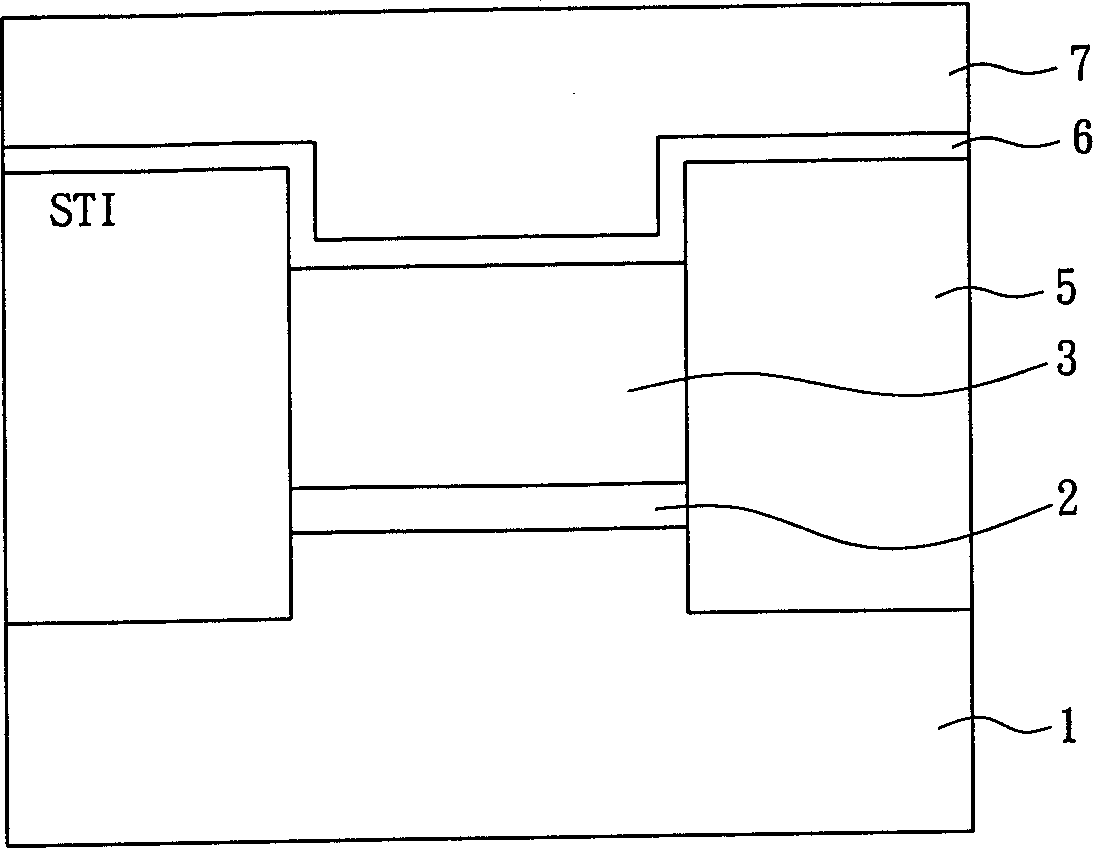
[0013] A method for manufacturing a flash memory, the steps are as follows: provide a semiconductor substrate 8, sequentially form a tunnel oxide layer 9 and a first conductive layer 10, and then form shallow trench isolation 11 (Shallow trench isolation; ST1), In this way, the front-end process has been completed, wherein the first conductive layer 10 is one of polysilicon, metal silicide or amorphous silicon, and its thickness is between 1000 Å and 5000 Å. Of course, as is well known in the industry, the front-end process can also be implemented in a different sequence, for example: first forming shallow trench isolation (STI) on the semiconductor substrate, and then sequentially depositing a tunnel oxide layer 9 and the first conductive layer 10 .

[0014] The key point of the present invention is to remove part of the first conductive layer 10, so that the shallow trench isolation 11 (STI) is higher than the first conductive layer 10, to facilitate subsequent process requir...


PUM


Abstract

The manufacture of flash memory includes providing a prefabricated semiconductor substrate with tunnel oxide layer and the first conductor layer on the oxide layer; removing partial first conductor layer to make the separating part in the shallow ditch higher than the first conductor layer; depositing one dielectric layer and etchbacking in the first conductor layer to form spacer as etching shield and etching the first conductor layer to form one channel; removing partial shallow ditch isolation to expose the outer side of the ditch; removing the spacer to form one floating gate; depositing a thin dielectric layer and the second conductor layer; and making pattern in the second conductor layer of form control gate.

Description

(1) Technical field [0001] The invention relates to a method for manufacturing a flash memory, in particular to a method for manufacturing a stacked gate flash memory that can provide a high capacitive coupling ratio. (2) Background technology [0002] Read Only Memory (Read Only Memory) is referred to as ROM for short, and the memory or data stored in ROM will not disappear due to power supply interruption, so it is also called Non-Volatile Memory (Non-Volatile Memory). With continuous improvement of non-volatile memory, flash memory (flash memory) has been developed. Flash memory (flash memory) has two operations of electrical program (electrical program) and electrical erase (electrical erase). Generally speaking, flash memory is composed of memory cell array (memory cell array) and peripheral circuit. Among them, the flash memory cell array used as data storage is composed of many memory cells arranged neatly on word lines interlaced with the array. line) and bit line ...

Claims


Application Information

Patent Timeline
IPC IPC(8): H01L21/8246H01L21/8247
Inventor 曾鸿辉
Owner VANGUARD INTERNATIONAL SEMICONDUCTOR CORPORATION
Why Eureka
Try Eureka