Method for mfg. multilayer printed wiring board and multilayer printed wiring board thereby

A multi-layer printing and circuit board technology, which is applied in the fields of printed circuit manufacturing, multi-layer circuit manufacturing, printed circuit, etc., can solve problems such as difficulty in providing chips

Inactive Publication Date: 2002-05-01
NITTO DENKO CORP
View PDF0 Cites 7 Cited by
  • Summary
  • Abstract
  • Description
  • Claims
  • Application Information

AI Technical Summary

Problems solved by technology

However, even the synthesis method is still difficult to provide low profile, light weight and high density wiring chips

Method used


Image

  • Method for mfg. multilayer printed wiring board and multilayer printed wiring board thereby
  • Method for mfg. multilayer printed wiring board and multilayer printed wiring board thereby
  • Method for mfg. multilayer printed wiring board and multilayer printed wiring board thereby

Examples


example 1

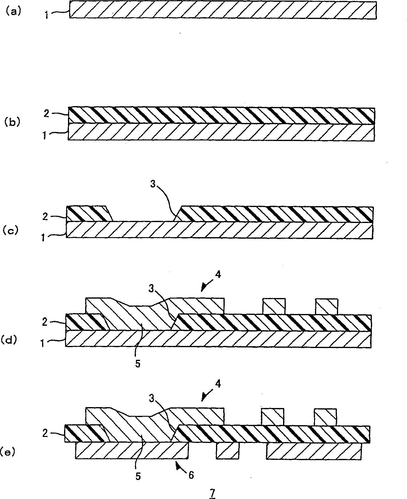
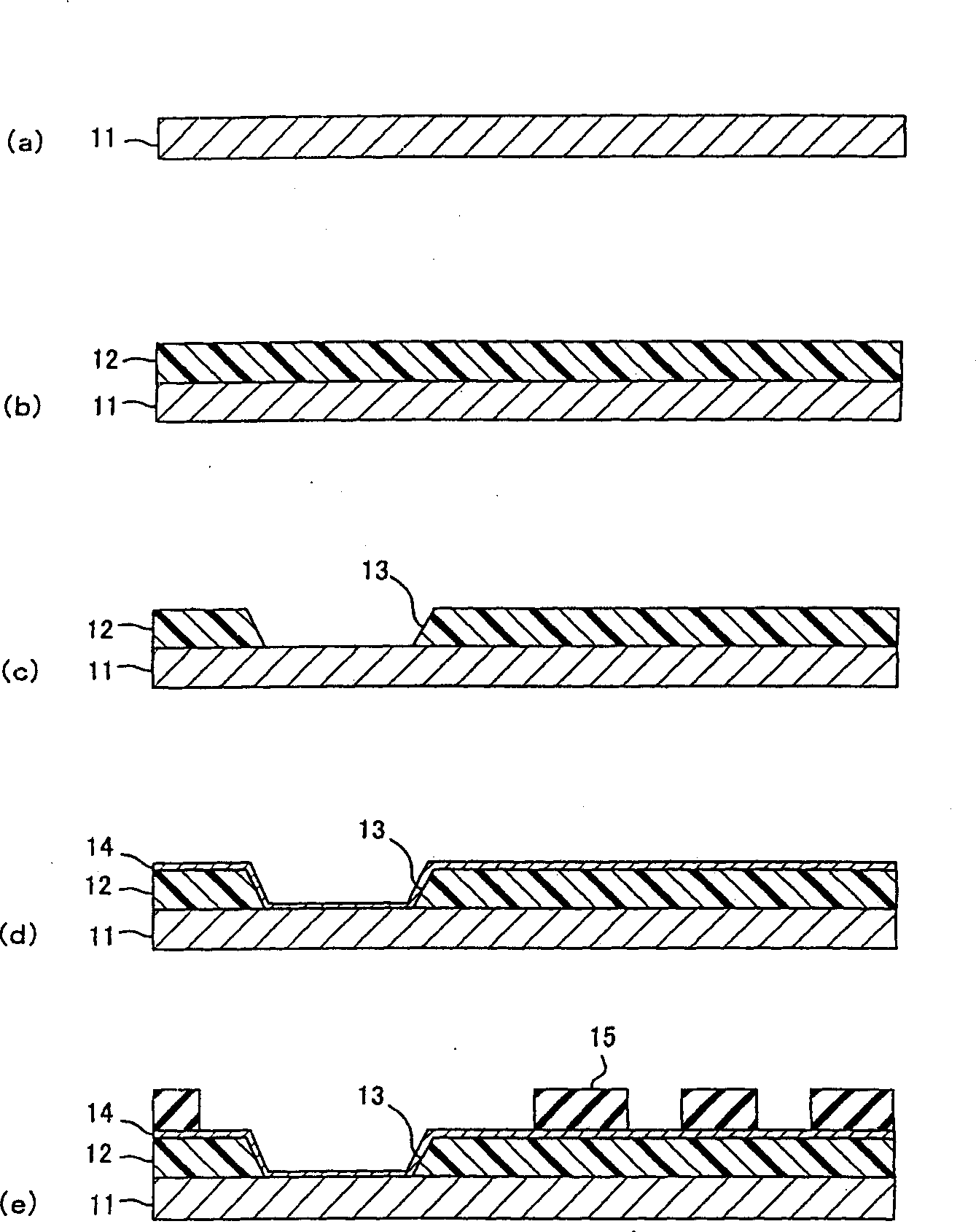
[0084] (manufacturing of double-sided substrates)

[0085] First, a rolled nickel foil (Ni-H available from Toyo Seihaku Co., Ltd.) with a thickness of 25 μm was cut to the desired size, and degreased (50ml / L-Metaclea CL-5513 available from Dai- ichiKogyo Seiyaku Co., Ltd.) at a temperature of 60°C for 2 minutes. Then rinse with water and dry. Through these steps, the nickel foil is ready, as figure 2 (a) shown. Subsequently, a photosensitive clear ink (BL-9700 available from Hitachi Chemical Co., Ltd.) was applied to one side of the nickel foil 11 by screen printing with a polyester mesh of 200 grids / inch. . Subsequently, it was placed in a desiccator at 80° C. for 40 minutes to dry. Through these steps, the insulating resin layer 12 with a thickness of about 30 microns is made, as figure 2 (b).

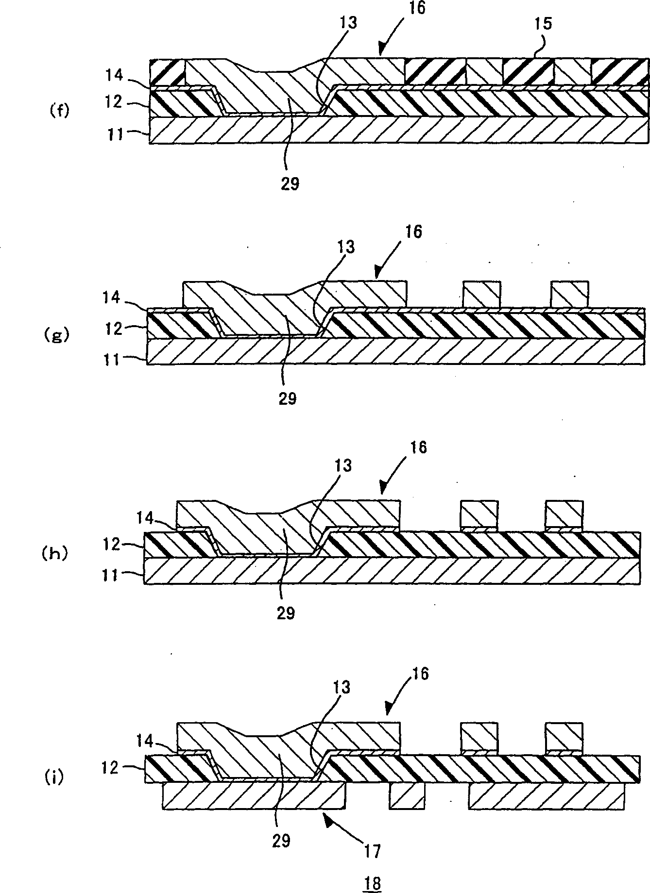
[0086] Next, after putting the mask in close contact with the insulating resin layer 12, use 2.7J / cm2 released from the ultra-high pressure mercury vapor lamp 2 of ultravi...

example 2

[0101] (Double-sided substrate manufacturing)

[0102] First, a rolled copper alloy foil (C-7025 available from Yamaha-Olin Metal Corporation) with a thickness of 35 micrometers was cut to the required size and degreased with a 60°C degreaser (200ml / L-OPC Acidclean 115 available from Okuno Chemical Industries Co., Ltd.) was treated for 2 minutes. Afterwards, wash with water and dry. Through these steps, the copper alloy foil 31 is prepared as Image 6 (a) shown.

[0103] Subsequently, the copper alloy foil 31 was immersed in 100 ml / L hydrochloric acid at 30° C. for 20 seconds, and then immersed in a palladium substitution plating solution (200 ml / L-ICP Accela available from Okuno Chemical Industries Co., Ltd.) at 30° C. for 3 minutes . Afterwards, wash with water. Again, it was immersed in a 60° C. electroless nickel plating solution (B-1 available from Meltex, Inc.) for 2 minutes, and then washed with water and dried. Through these steps, a nickel plating layer 32 with ...

example 3

[0118] In addition to the rolled nickel foil with a thickness of 25 microns (Ni-H is available from Toyo Seihaku Co., Ltd.), the rolled SUS304 foil with a thickness of 25 microns (SUS304H-TA is available from Toyo Seihaku Co., Ltd. .obtained) can also be used as a metal foil, the same method in Example 1 can be used to manufacture a double-sided substrate, and then the same method in Example 1 is used to manufacture a 4-layer printed wiring board by using the double-sided substrate.


PUM

PropertyMeasurementUnit
thicknessaaaaaaaaaa
thicknessaaaaaaaaaa
thicknessaaaaaaaaaa

Abstract

To provide a method of producing a multilayer printed wiring board that can be intended to have low-profile, light-weight and high-density wiring of a printed wiring board, and a multilayer printed wiring board produced by the method of producing a multilayer printed wiring board, the double-sided substrate is produced by the steps of forming an insulating resin layer on a metal foil; of forming a via hole in the insulating resin layer; of forming a first circuit pattern on the insulating resin layer and forming a conductive layer in the via hole, by plating; and of etching the metal foil to form it into a second circuit pattern. The produced double-sided substrate is used as a core substrate for producing multilayer printed wiring board by a laminate-en-bloc or a build-up method.

Description

technical field [0001] The invention relates to a method for manufacturing a multilayer printed circuit board and a multilayer printed circuit board manufactured by using the method for manufacturing a multilayer printed circuit board. Background technique [0002] In general, methods of manufacturing multilayer printed wiring boards can be roughly classified into two typical methods. One is lamination integration. In this method, multiple double-sided substrates are used as core substrates, which can have prescribed circuit patterns on both sides, and are laminated and bonded on the entire prepreg through prepreg. The other is a synthesis method in which prescribed circuit patterns and insulating resin layers are sequentially formed. [0003] In the lamination method, a substrate, such as a copper-clad laminate, is formed by laminating copper foil on a fabric or glass nonwoven or aramid impregnated with epoxy or phenolic resin, which is used as a chip use. Holes formed i...

Claims


Application Information

Patent Timeline
Patent Type & Authority Applications(China)
IPC IPC(8): H05K1/09H05K3/10H05K3/38H05K3/42H05K3/46
CPCH05K2201/09563H05K3/108H05K3/4602H05K2201/0344H05K3/4644H05K3/4623H05K3/423H05K3/388H05K2201/0355H05K2201/0394H05K1/09Y10T29/49156Y10T29/49117Y10T29/49165Y10T29/49126Y10T29/49155Y10T29/49128
Inventor 諏訪時人田中厚谷川聡藤井弘文宗和範
Owner NITTO DENKO CORP
Why Eureka
Try Eureka