Electrically erasable molecular base organic electric bistable film device and its producing technology

A thin-film device and manufacturing process technology, which is applied in the field of molecular-based electric bistable thin film devices and its manufacturing process, can solve the problems of few times of erasing and writing, small contrast between the two states, and difficulty in erasing and writing, and achieve a large number of switching times , the effect of large state contrast

Inactive Publication Date: 2002-06-05
FUDAN UNIV
View PDF0 Cites 14 Cited by
  • Summary
  • Abstract
  • Description
  • Claims
  • Application Information

AI Technical Summary

Problems solved by technology

[0004] In molecular electronic devices, the reversible switching of molecular switches is a big problem, that is, it is difficult to erase and write with electricity
Even if a few ex

Method used


Image

  • Electrically erasable molecular base organic electric bistable film device and its producing technology
  • Electrically erasable molecular base organic electric bistable film device and its producing technology

Examples


Embodiment Construction

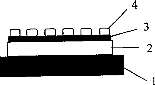
[0039] The basic structure and performance of the present invention will be described below by taking IMCN as an example.

[0040] On the clean slide surface, make a layer of Ag film with vacuum thermal evaporation method as the bottom electrode, then vapor-deposit a layer of thickness and be 80-120 nanometer IMCN, vapor-deposit many Al spots on the organic film again as the top electrode ( Each Al spot is equivalent to a top electrode, and the area of ​​each top electrode is 0.05-2 square millimeters), thus a kind of thin film device Ag-IMCN-Al is obtained.

[0041] The electrical bistable characteristics of the thin film device Ag-IMCN-Al were measured, and the results are as follows:

[0042] The initial resistance of the thin film device is greater than 20 megohms. After turning into a low resistance state, the resistance value is 20-100 ohms, and after returning to a high resistance state, the resistance value is 10 kohms to 5 megohms, and the contrast between the two st...


PUM


Abstract

The invention relates to an electricity bistable film device that is based on molecularity and wide electricity rewritable capability. The device is a samdwich structure composed of bottom electrode,top electrode and organic molecular film. The thin film device can be manufactured by using vacuum thermal steam-plasting. The device provides features that erasting and writing times reach to 10-1000; contrast of two states in more than 1000 times; one writing time is less than 100 nanoseconds; one erasting time is less than 1 microsecond. The invented bistable thin film can be used to develop electricity erasing and writing storing device with super high density, molecularity logic gate and over-voltage protector.

Description

technical field [0001] The invention belongs to the technical field of molecular electronic devices, and in particular relates to an electrically rewritable molecular-based bistable thin film device and a manufacturing process thereof. technical background [0002] The development trend of electronic devices and integrated circuits is smaller size, faster speed and lower power consumption. Considering that traditional silicon-based semiconductors need a certain scale to maintain solid properties, coupled with the limitations of lithography, doping and other process technology conditions, the size of microelectronic components will reach the limit. Therefore, it is necessary to develop new functional materials and develop corresponding manufacturing technologies. [0003] The use of organic functional molecules to fabricate molecular devices and integrated circuits is a feasible solution. This is due to the small interaction volume of organic molecules (which can in princip...

Claims


Application Information

Patent Timeline
IPC IPC(8): H01L51/30H01L51/40
Inventor 徐伟吕银祥华中一
Owner FUDAN UNIV
Why Eureka
Try Eureka