
Magnetic RAM of transistor with vertical structure and making method thereof

A random access memory, vertical structure technology, used in semiconductor/solid state device manufacturing, static memory, digital memory information, etc., can solve the problems of unit operation influence, difficult resistance control, etc.

Inactive Publication Date: 2002-12-18
SK HYNIX INC
View PDF0 Cites 40 Cited by
  • Summary
  • Abstract
  • Description
  • Claims
  • Application Information

AI Technical Summary

Problems solved by technology

However, as the transistor size gets smaller, the resistance is more difficult to control, and the resistance of the transistor together with the resistance of the MTJ cell has a large impact on the operation of the cell

Method used


Image

  • Magnetic RAM of transistor with vertical structure and making method thereof
  • Magnetic RAM of transistor with vertical structure and making method thereof
  • Magnetic RAM of transistor with vertical structure and making method thereof

Examples


Embodiment Construction

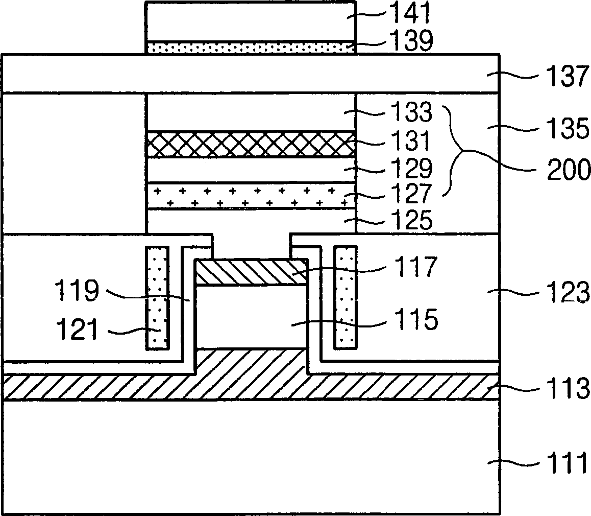
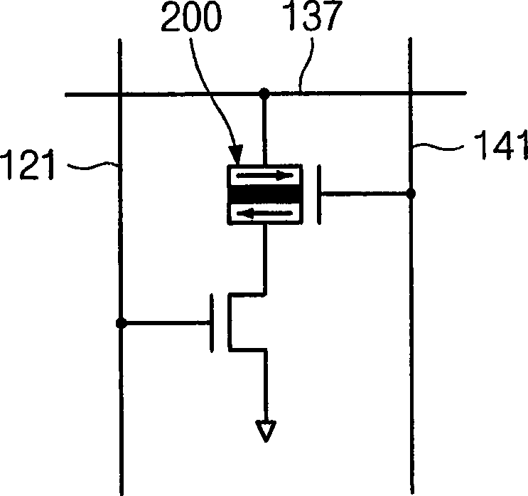
[0025] Exemplary embodiments are shown in Figure 2A-5 , Figure 2A , 2B 2C and 2C represent a cross-sectional view, a circuit diagram and a top plan view, respectively, of an MRAM with vertically structured transistors according to an embodiment.

[0026] see Figure 2A , the MRAM has a vertically structured transistor including a source junction region 113 formed over a semiconductor substrate 111 including a column 115 . The vertical structure transistor also includes a drain junction region 117 formed in the cylinder 115 and located at the center of the source junction region 113 . A gate oxide layer 119 is formed over the surface of the substrate 111 at the outer surface of the sidewall of the cylinder 115 , and the gate electrode 121 is formed on the outer surface of the gate oxide layer 119 . Such as Figure 2C As shown, gate oxide layer 119 and gate electrode 121 are preferably formed around the entire circumference of cylinder 115 .

[0027] The vertical structu...


PUM


Abstract

The invention discloses a magnetic random access memory with a vertical structure transistor, which has faster access time than SRAM, high density similar to DRAM and non-volatile characteristics similar to flash memory. The magnetic random access memory comprises a vertical structure transistor, a first word line including the transistor, a contact line connected to the transistor, a magnetic tunnel junction unit deposited on the contact line, and a magnetic tunnel junction unit formed on the magnetic tunnel junction unit bit line, and a second word line formed on the bit line at the position of the magnetic tunnel junction cell. Through the disclosed structure, while using a simplified manufacturing process, the integration density of semiconductor devices can be increased, the short channel effect can be improved, and the control rate of resistance can be improved.

Description

technical field [0001] The present invention relates to a kind of magnetic random access memory (hereinafter referred to as MRAM) with vertical structure transistor, relate in particular to a kind of MRAM, it has faster access time than SRAM (static random access memory), and DRAM (dynamic random access memory) access memory) similar high density and flash memory similar non-volatility. Background technique [0002] As one of next-generation memories, some semiconductor memory manufacturers have proposed MRAMs using ferromagnetic materials. MRAM is a type of memory that reads and writes information by forming multiple layers of ferromagnetic thin films and detecting changes in current depending on the magnetization direction of each thin film. The MRAM device has high speed and low power consumption, and it allows a high degree of integration due to the special properties of the magnetic thin film. Similar to flash memory, it also performs non-vol...

Claims


Application Information

Patent Timeline
Patent Type & Authority Applications(China)
IPC IPC(8): G11C11/14G11C7/02G11C8/00G11C11/00G11C11/15G11C11/16H01L21/00H01L21/822H01L21/8246H01L27/105H01L27/22H01L29/76H01L29/94H01L31/062H01L31/113H01L31/119H01L43/08
CPCB82Y10/00G11C11/161H10B61/22H01L27/105
Inventor 车宣龙
Owner SK HYNIX INC
Learn More