Production method for copper-clad laminated sheet

A technology of copper clad laminate and manufacturing method, which is applied in the direction of multi-layer circuit manufacturing, lamination, lamination device, etc., can solve the problems of reducing the utilization rate of raw materials of products and deterioration of etching accuracy, etc.

Inactive Publication Date: 2002-12-18
MITSUI MINING & SMELTING CO LTD
View PDF0 Cites 9 Cited by
  • Summary
  • Abstract
  • Description
  • Claims
  • Application Information

AI Technical Summary

Problems solved by technology

That is to say, the etching accuracy of the outer layer copper foil directly above the formed interstitial via hole (IVH) or blind via hole (BVH) will immediately deteriorate, thereby greatly reducing the raw material utilization rate of the product

Method used


Image

  • Production method for copper-clad laminated sheet
  • Production method for copper-clad laminated sheet
  • Production method for copper-clad laminated sheet

Examples


Embodiment 1

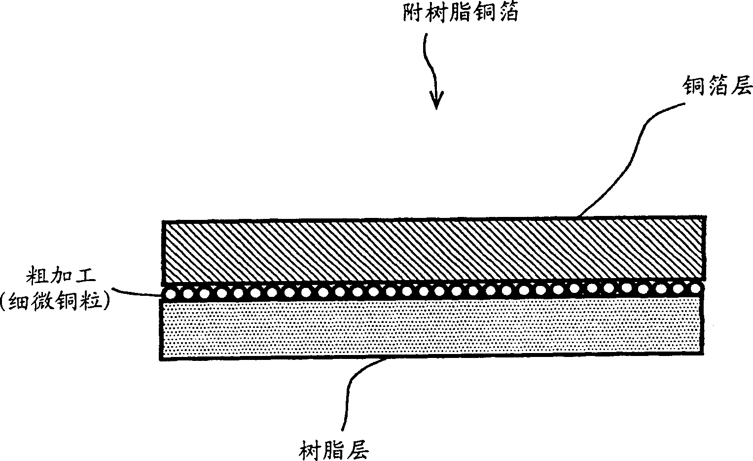
[0041] Here, the copper foil of claim 1 is used, that is, a VLP copper foil classified as a very low profile type foil with a thickness of 18 micrometers according to the IPC standard. The characteristic of this VLP copper foil is that the tensile strength is 52 kg / mm 2 , Vickers hardness is 150, the elongation after heating is 3.8%, the breaking strength measured by the pressure test after heating is 552 kN / m 2 .

[0042] A resin layer 3 with a thickness of 50 microns is formed on the rough surface of the VLP copper foil with fine copper particles 2 attached to form the copper foil 4 with resin. When forming the resin layer 3, use the following chemical reagents to dissolve in methyl ethyl ketone to form a resin composition with a solid content of 45%: bisphenol A epoxy resin (trade name: 60% by weight) EPOMIC R-301, manufactured by Mitsui Petrochemical Co., Ltd.), 20% by weight of rubber-modified epoxy resin (trade name: EPOTHOTOYR-102, manufactured by Toto Kasei Co., Ltd.) of 2...

Embodiment 2

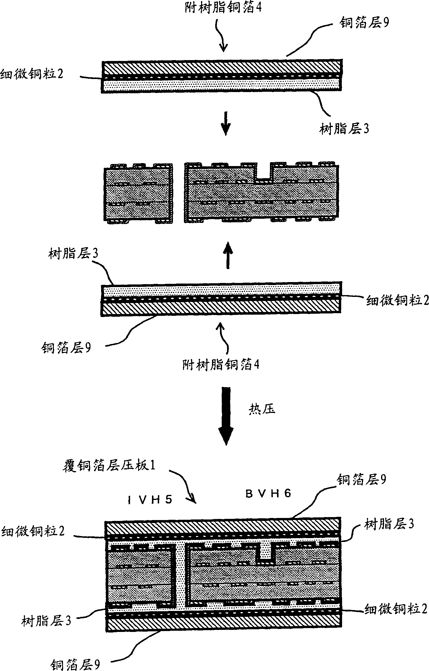
[0046] Here, the copper foil described in claim 2 is used, that is, the copper foil 10 with an etchable carrier foil, which is formed on the side surface of the aluminum carrier foil 8 with a thickness of 25 μm to form a copper foil circuit with a thickness of 3 μ. Foil layer 9. For the following parts that are the same as in the first embodiment, in order to avoid repetition, this description is omitted. In addition, the same parts are represented by the same symbols as in the first embodiment as much as possible.

[0047] A resin layer 3 with a thickness of 100 microns is formed on the surface of the rough-processed copper foil layer 9 with fine copper particles 2 attached to the copper foil with a carrier 10 to form a carrier foil with the resin layer Copper foil 11. At this time, the resin used for forming the resin layer 3 is the same as in the case of the first embodiment, so the description is omitted.

[0048] Then, use this copper foil 11 with a resin layer attached to Fi...

Embodiment 3

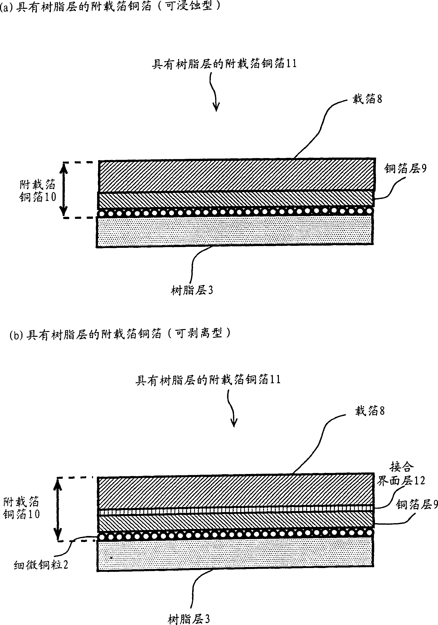
[0050] Here, the copper foil of claim 3, that is, the copper foil 10 with a peelable carrier foil, is formed on the side surface of the 18 micron thick copper carrier foil 8 to form a copper foil corresponding to a thickness of 5 μ to form a copper foil circuit. Layer 9, and the bonding interface layer 12 is formed between the carrier foil layer 8 and the copper foil layer 9 with carboxy benzotriazole. For the following parts that are the same as in the first embodiment, in order to avoid repetition, this description is omitted. In addition, the same parts are represented by the same symbols as in the first embodiment as much as possible.

[0051] A resin layer 3 with a thickness of 100 microns is formed on the surface of the rough-processed copper foil layer 9 with fine copper particles 2 attached to the copper foil with a carrier 10, thereby forming a carrier foil with the resin layer Copper foil 11. At this time, the resin used to form the resin layer 3 is the same as in the case...


PUM

PropertyMeasurementUnit
thicknessaaaaaaaaaa
thicknessaaaaaaaaaa
thicknessaaaaaaaaaa

Abstract

The object of the present invention is to prevent the sag caused when the outer copper foil layer is attached to the substrate for the inner layer, wherein the substrate for the inner layer has an interlayer conduction device such as an interstitial via hole (IVH) or a blind via hole (BVH). holes or recesses. For this reason, the manufacturing method of the copper-clad laminate adopted is characterized in that the following copper foil is used as the outer layer to make the copper-clad laminate: (1) The breaking strength measured by the compression test after heating is 275 kN Resin-attached copper foil with a resin layer formed on the surface of copper foil with a thickness of 15 microns or more per square meter, (2) copper foil with an erodible carrier foil, and the total thickness of the carrier foil layer and the copper foil layer is or (3) copper foil with peelable carrier foil, wherein the total thickness of the carrier foil layer and the copper foil layer is more than 20 microns, and the thickness formed between the carrier foil layer and the copper foil layer is measured after heating. The peeling thickness of the bonding interface layer is 5-300 grams force (gf)/cm.

Description

[0001] The technical field of the invention [0002] The invention relates to a method for manufacturing a copper clad laminate. Background technique [0003] In the past, as a device for obtaining interlayer conduction between the inner circuit layers of a multilayer printed circuit board, a through hole as an interstitial via hole (IVH) or as a blind through hole on the inner circuit board can be used. Devices such as blind via hole (BVH). These interlayer conduction devices can form fine circuits of printed circuit boards and are widely used as high-density packaging devices. [0004] The copper clad laminates or printed circuit boards with interlayer conduction devices such as these gap through holes (IVH) and blind through holes (BVH) are manufactured by the build-up process, in which the copper foil is repeated many times It is attached to the outer layer of the printed circuit board as the core material to finally form the inner layer circuit, thereby forming a copper foil c...

Claims


Application Information

Patent Timeline
Patent Type & Authority Applications(China)
IPC IPC(8): B32B15/08H05K1/09H05K3/02H05K3/46
CPCB32B15/08B32B37/0023B32B2311/12B32B2457/08H05K1/09H05K3/025H05K3/4602H05K3/4652H05K2201/0355H05K2201/0358H05K2201/09509Y10S428/914Y10T428/1438Y10T428/24843Y10T428/24917Y10T428/2804H05K3/38B32B15/20
Inventor 桑子富士夫石野友宏
Owner MITSUI MINING & SMELTING CO LTD
Why Eureka
Try Eureka