Anode oxidizing process for treating surface of porous silicon
A technology of anodic oxidation and surface treatment, applied in post-processing, post-processing details, chemical instruments and methods, etc., can solve the problems of difficult control accuracy, unsuitable for industrial production, complex equipment, etc., easy to achieve accuracy control, and low production cost , the effect of simple equipment
- Summary
- Abstract
- Description
- Claims
- Application Information
AI Technical Summary
Problems solved by technology
Method used
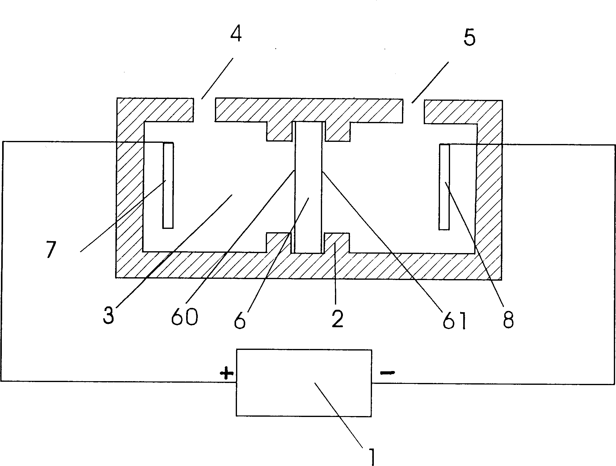
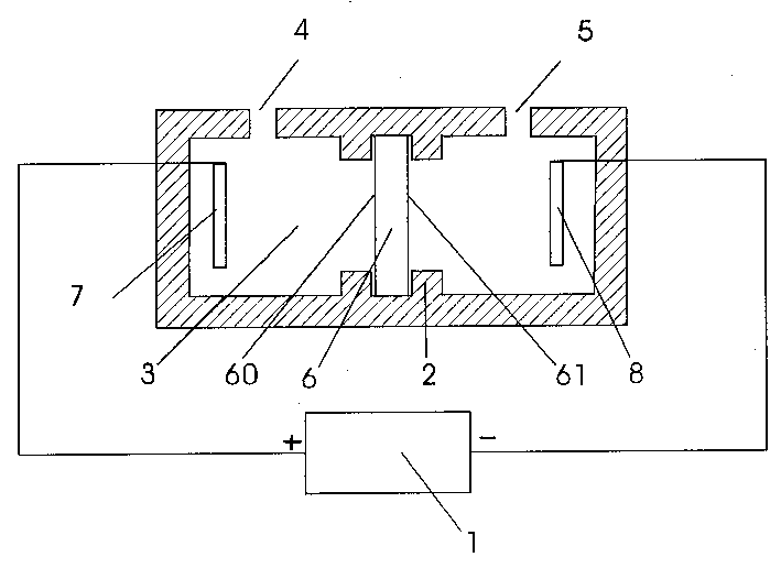
Image

Examples
Embodiment 1
[0019] The anodic oxidation surface treatment technology of embodiment 1 porous silicon
[0020] Porous silicon anodized surface treatment process: H 2 o 2 Solution concentration: 0.5%
[0021] Voltage of regulated power supply 1: 2.2v
[0022] Current density: 0.5mAcm -2
[0023] Power-on time: 20min
[0024] Drying process: cleaning time: 12min
Embodiment 2
[0026] The anodic oxidation surface treatment technology of embodiment 2 porous silicon
[0027] Porous silicon anodized surface treatment process: H 2 o 2 Solution concentration: 10%
[0028] Voltage of regulated power supply 1: 2.6v
[0029] Current density: 3mAcm -2
[0030] Power-on time: 10min
[0031] Drying process: cleaning time: 15min
[0032] Drying method: one of four drying methods
Embodiment 3
[0033] The anodic oxidation surface treatment technology of embodiment 3 porous silicon
[0034] Porous silicon anodized surface treatment process: H 2 o 2 Solution concentration: 24%
[0035] Voltage of regulated power supply 1: 4.8v
[0036] Current density: 9mAcm -2
[0037] Power-on time: 50sec
[0038] Drying process: cleaning time: 18min
[0039] Drying method: one of four drying methods
[0040] The above embodiments greatly weaken the surface activity of the porous silicon, making it possible to dry the wet porous silicon by any conventional drying method.
[0041] So far, a dry porous silicon product is obtained.
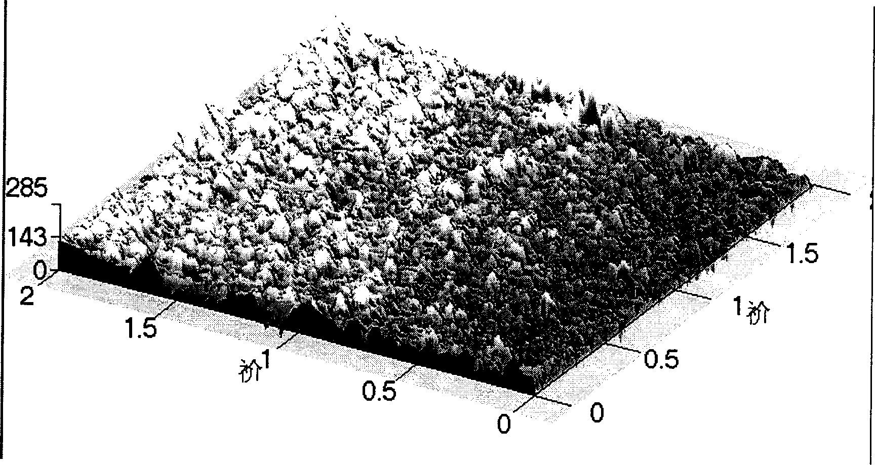
[0042] The porous silicon treated by one of the anodic oxidation surface treatment techniques in Examples 1 to 3, after being dried by a conventional drying method, has a smooth surface and is as bright as a mirror, and can be stored in the air for a lo...
PUM
| Property | Measurement | Unit |
|---|---|---|
| Current density | aaaaa | aaaaa |
| Current density | aaaaa | aaaaa |
| Current density | aaaaa | aaaaa |
Abstract
Description
Claims
Application Information