InGaAs/InP PIN photo electric detector and its manufacturing technology

A technology for photodetectors and manufacturing processes, applied in sustainable manufacturing/processing, photovoltaic power generation, electric solid-state devices, etc., can solve problems such as high cost, large dark current, and low responsivity

Inactive Publication Date: 2003-04-30
XIAMEN UNIV
View PDF0 Cites 16 Cited by
  • Summary
  • Abstract
  • Description
  • Claims
  • Application Information

AI Technical Summary

Problems solved by technology

[0005] To sum up, the existing InGaAs/InP PIN photodetectors have problems such as large dark current, lo...

Method used


Image

  • InGaAs/InP PIN photo electric detector and its manufacturing technology
  • InGaAs/InP PIN photo electric detector and its manufacturing technology
  • InGaAs/InP PIN photo electric detector and its manufacturing technology

Examples


Embodiment Construction

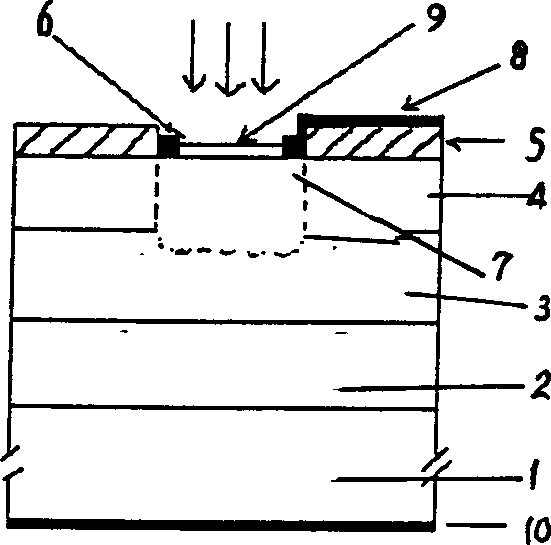
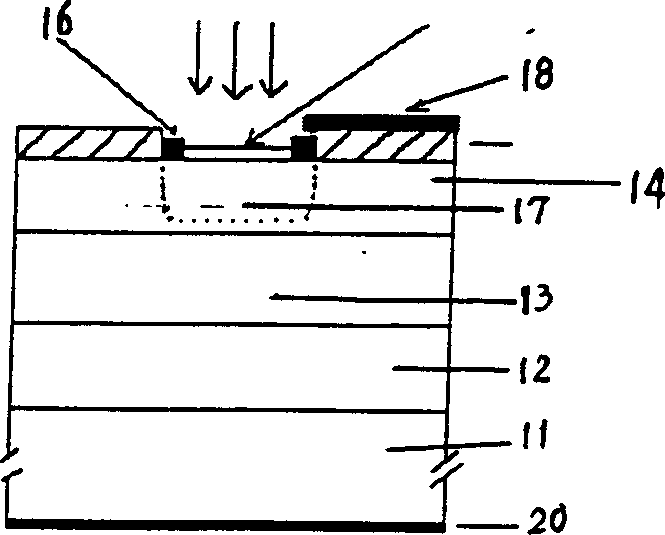
[0051] Such as figure 2 Shown, the new structure of the InGaAs / InP PIN photodetector that the present invention adopts is:

[0052] i-InP top layer 14 / i-In 0.53 Ga 0.47 As photosensitive layer 13 / i-InP buffer layer 12 / N + -InP substrate 11 four-layer double heterojunction material structure. Direct evaporation of Al on i-InP top layer 14 2 o 3 passivation film 19, and a diffusion window 16 is photoetched, and the i-InP top layer in the window is made P + Zinc expansion, so that the diffusion region 17 is close to the i-In 0.53 Ga 0.47 As photosensitive layer 13, in the diffusion window and Al 2 o 3 Evaporate Au / Zn and Ti / Al on the passivation film and photoetch the incident light window and P-type ohmic contact electrode 18 . The bottom layer is an N-type ohmic contact layer 20, which adopts an AuGeNi alloy layer.

[0053] The fabrication process flow of InP / InGaAs / InP PIN photodetector is described as follows.

[0054] Prepare epitaxial wafers gro...


PUM


Abstract

A InGaAs/InP PIN photoelectric detector relating to a semiconductor component has the structure of double hetergeneous material in four layer of i-In0.53 Ga 0.47As photosensitive layer/i-InP buffer layer/N+-Inp substrate. There is P+ zinc diffusion layer which is close to i-In 0.53 Ga0.47 As photosensitive layer but not reach the photosensitive layer at the top layer. It is prepared by the following steps, growing a passivation film of aluminium oxide on the epitaxial sheet and carrying out open-type zinc diffusion by using zinc as a diffusion source, depositing high quality film of aluminiumoxide on InP material by directly using evapouration to reduce dark current, and raising the signal to noise ratio. The film obtained can be used in passivation film of InP material.

Description

(1) Technical field [0001] The invention relates to a semiconductor device, in particular to an InGaAs / InP PIN photodetector for converting optical signals into electrical signals and its manufacturing process. (2) Background technology: [0002] Photodetectors are semiconductor devices that convert optical signals into electrical signals, and are used in optical fiber communications, computer networks, cable TV networks, and various photoelectric control and photodetection systems. Photodetectors mainly have two structures: PIN and APD (Avalanche Diode). The former only detects and does not amplify, and usually works under -5V reverse bias; the latter detects and amplifies at the same time, and must work under high bias. InGaAs / InP materials are generally used for photodetectors working at long wavelengths of 1310-1550nm. PIN photodetector works under low voltage, has high responsivity, good signal-to-noise ratio, and is easy to use. It is the most commonly used photodete...

Claims


Application Information

Patent Timeline
IPC IPC(8): H01L27/14H01L31/105H01L31/18
CPCY02E10/50Y02P70/50
Inventor 陈朝刘宝林
Owner XIAMEN UNIV
Why Eureka
Try Eureka