Semiconductor storage device

A storage device and semiconductor technology, applied in the direction of information storage, static memory, digital memory information, etc., can solve the problems of shortening the storage unit time, reducing the writing time, small chip size, etc., and achieve chip size reduction and simplification of the structure , the effect of reducing the unit area

Inactive Publication Date: 2003-06-04
RENESAS ELECTRONICS CORP
View PDF2 Cites 6 Cited by
  • Summary
  • Abstract
  • Description
  • Claims
  • Application Information

AI Technical Summary

Problems solved by technology

[0029] In view of the foregoing, an object of the present invention is to provide a semiconductor memory device that does not slow down normal read / write access due to the influence of the update, and does not cause access delay even when there is a skew phenomenon in the address. In order to solve problems such as damage to the memory cell, by reducing the writing time, the overall time of the memory cell can be shortened, and even when the general-purpose SRAM standard is operated and the capacity is increased, the chip size is small, the power consumption is low, and an inexpensive semiconductor is provided. storage device

Method used


Image

  • Semiconductor storage device
  • Semiconductor storage device
  • Semiconductor storage device

Examples


no. 1 Embodiment approach

[0067] Hereinafter, embodiments of the present invention will be described with reference to the drawings. [first embodiment]

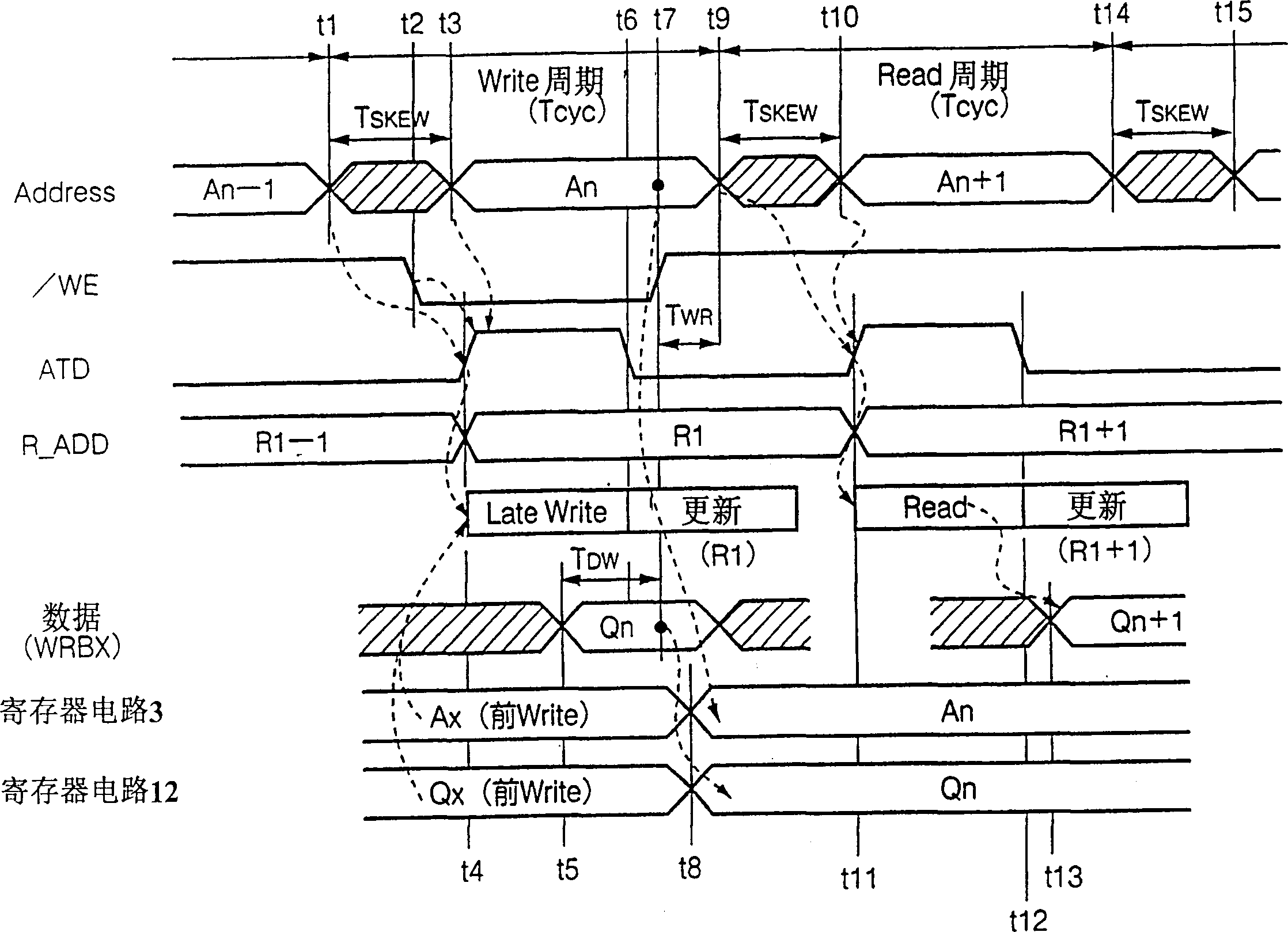
[0068] First, the present embodiment will be briefly described. As described in the first related art to the third related art above, if reading and writing corresponding to external access requests are performed after updating, the address access time T AA Increase. Therefore, in this embodiment, when there is an access request from the outside, the update is performed after reading or writing corresponding to the access request. However, relying solely on this, the problems pointed out in the third related art and the fourth related art also arise. Therefore, this embodiment implements a late write (Late Write) method to write to the memory cell, thereby shortening the writing time and storage cycle.

[0069] That is, in the storage cycle that is provided with an external write request, only the provided write address and write data are put int...

no. 2 Embodiment approach

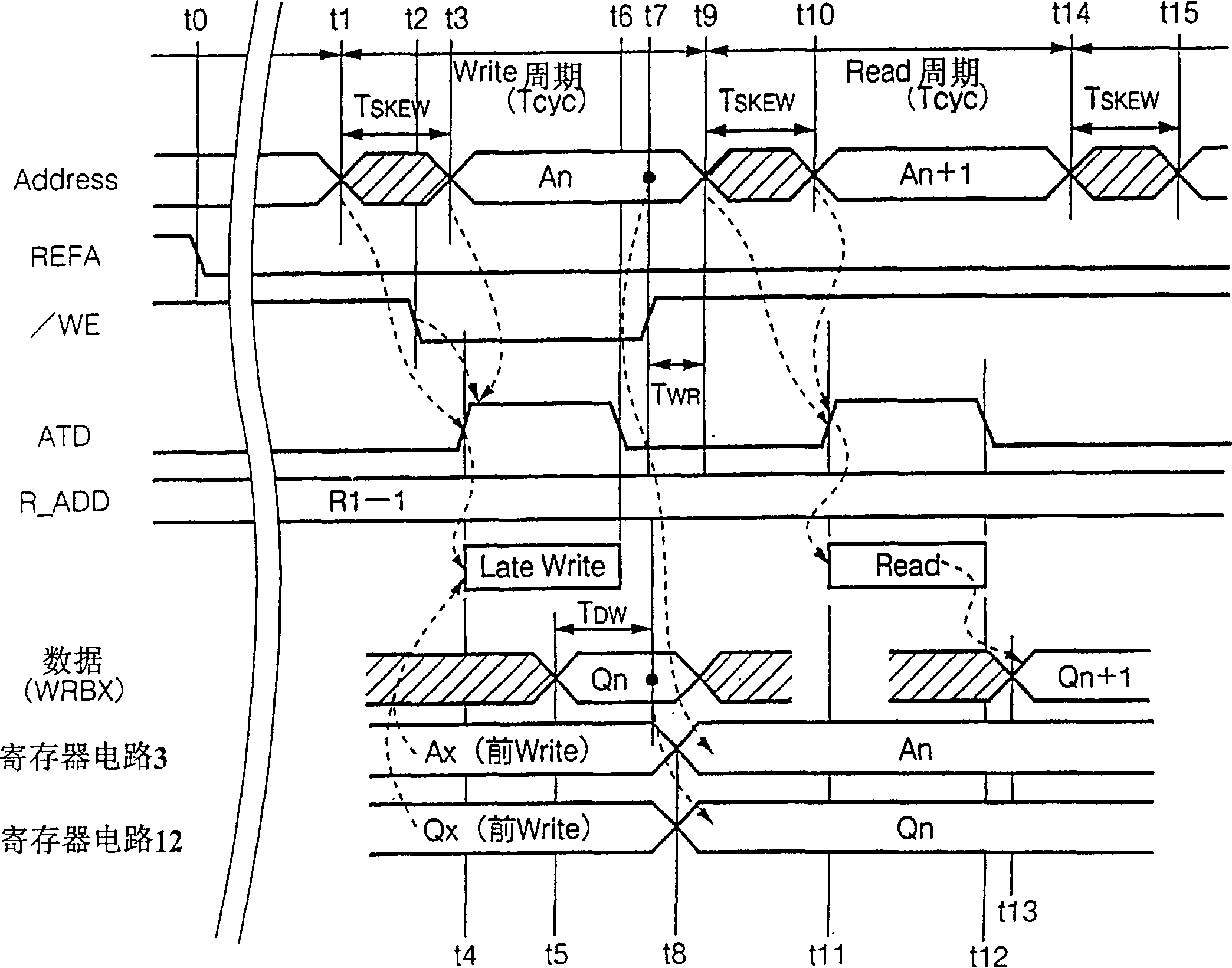
[0204] In the first embodiment, in one storage cycle (cycle time T cyc ) to perform delayed write and update or read and update. On the other hand, in this embodiment, for example, by performing two accesses (delayed writing or reading) and one update in two consecutive storage cycles, the cycle time is shortened compared with the first embodiment, in order to realize High speed.

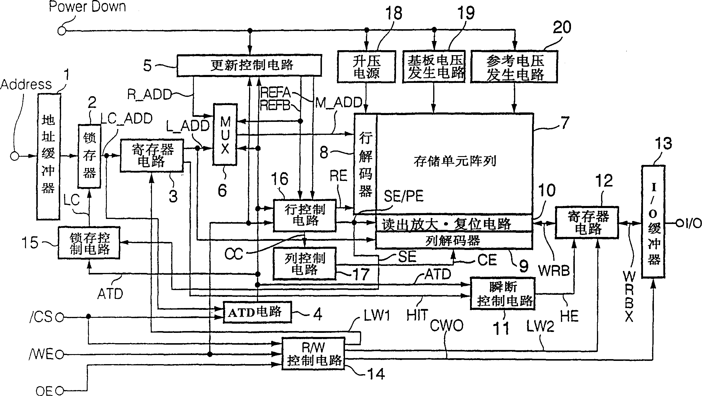
[0205] Figure 8 Shown is a block diagram showing the configuration of the semiconductor memory device according to the present embodiment, and the components and figure 1 The same use the same symbol. and figure 1 The difference is that the ATD circuit 4 is replaced by an ATD circuit 24 , and refresh control signals REFA, REFB are input to the ATD circuit 24 . As described below, the generation timing of the address change detection signal ATD in this embodiment is slightly different from that in the first embodiment.

[0206] That is, in the first embodiment, the ATD circuit 4 generates a po...

no. 3 Embodiment approach

[0215] In the first and second embodiments described above, the memory cycle is shortened by delaying writing. On the other hand, in this embodiment, the following conditions are added to the conditions of the first embodiment. In this way, instead of delaying writing as in the first embodiment, the actual writing to the memory cell is performed during the storage cycle with a write request, so that the advantages of shortening the storage cycle and the like can be obtained similarly to the first embodiment. Effect.

[0216] That is, in the first embodiment and the like, it is considered that the write data is determined later than the fall of the write enable signal / WE and after the address time lag period. In this embodiment, when determining the specifications of the semiconductor memory device, not only the write enable signal / WE but also the write data during the address skew period are taken into consideration. In this way, as in the case of delayed writing, the writ...


PUM


Abstract

A semiconductor storage device operating according to SRAM specifications in which normal access is not delayed by the effect of refresh and the memory cycle can be shortened as compared with conventional one. An ATD circuit (4) is subjected to variation of address (Address) and generates a one-shot pulse in an address variation detection signal (ATD) after an address skew period. In response to a write request, a write enable signal ( / WE) is caused to fall during the address skew period. Write or read is started at the rise of the one-shot pulse. When write is performed, late write is performed, using an address and data provided when write is requested immediately before. Subsequently, refresh is performed within a period from the fall of the one-shot pulse and to the end of the address skew period of the next memory cycle. For the late write performed in response to the next write request, an address and data are taken into register circuits (3, 12) at the rise of the write enable signal ( / WE).

Description

field of invention [0001] The present invention relates to a semiconductor memory device. The memory cell array is composed of the same memory cells as DRAM (Dynamic Random Access Memory), and when viewed from the outside of the semiconductor memory device, its operating specifications are the same as those of general-purpose SRAM (Static RAM). same. In particular, the present invention relates to a standby semiconductor storage device suitable for portable devices such as portable phones and PHS (Personal Handyphone System). Background technique [0002] As semiconductor devices capable of random access, the most representative ones are SRAM and DRAM. Compared with DRAM, SRAM is generally faster. As long as the power is supplied and the address is input, the change of the address can be captured, and the internal sequential logic circuit is activated to perform reading and writing. In this way, compared with DRAM, SRAM can operate only by providing a simple input signal w...

Claims


Application Information

Patent Timeline
Patent Type & Authority Applications(China)
IPC IPC(8): G11C11/403G11C7/10G11C11/401G11C11/406G11C11/407G11C11/408
CPCG11C11/406G11C11/40615G11C11/408G11C11/40
Inventor 高桥弘行稻叶秀雄中川敦
Owner RENESAS ELECTRONICS CORP
Why Eureka
Try Eureka