Insulative film etching device

An etching device and insulating film technology, applied in electrical components, semiconductor/solid-state device manufacturing, circuits, etc., can solve the problems of unstable substrate temperature, non-uniformity, promoting film accumulation, etc., to suppress productivity reduction and cleaning frequency. Less and more efficient cleaning

Inactive Publication Date: 2003-07-02
ANELVA CORP
View PDF0 Cites 7 Cited by
  • Summary
  • Abstract
  • Description
  • Claims
  • Application Information

AI Technical Summary

Problems solved by technology

Once the particles stick to the surface of the substrate, in addition to the abnormal shape of the etching, it may cause major defects such as open circuit and short circuit of the circuit.
In addition, if the peeled deposited film adheres to the substrate holding surface of the substrate holder, there will be a problem that the contact between the substrate and the substrate holding surface will be reduced during subsequent etching.
Once the contact between the substrate and the substrate holding surface decreases, the temperature of the substrate during etching is unstable and uneven, and the etching characteristics may deteriorate
[0008] Especially recently, in the background of miniaturization and high-functionality of products, gases with various functions are added and used, and film deposition may be promoted due to the influence of added gases

Method used


Image

  • Insulative film etching device
  • Insulative film etching device
  • Insulative film etching device

Examples


Embodiment Construction

[0033] Next, examples of the present invention will be described.

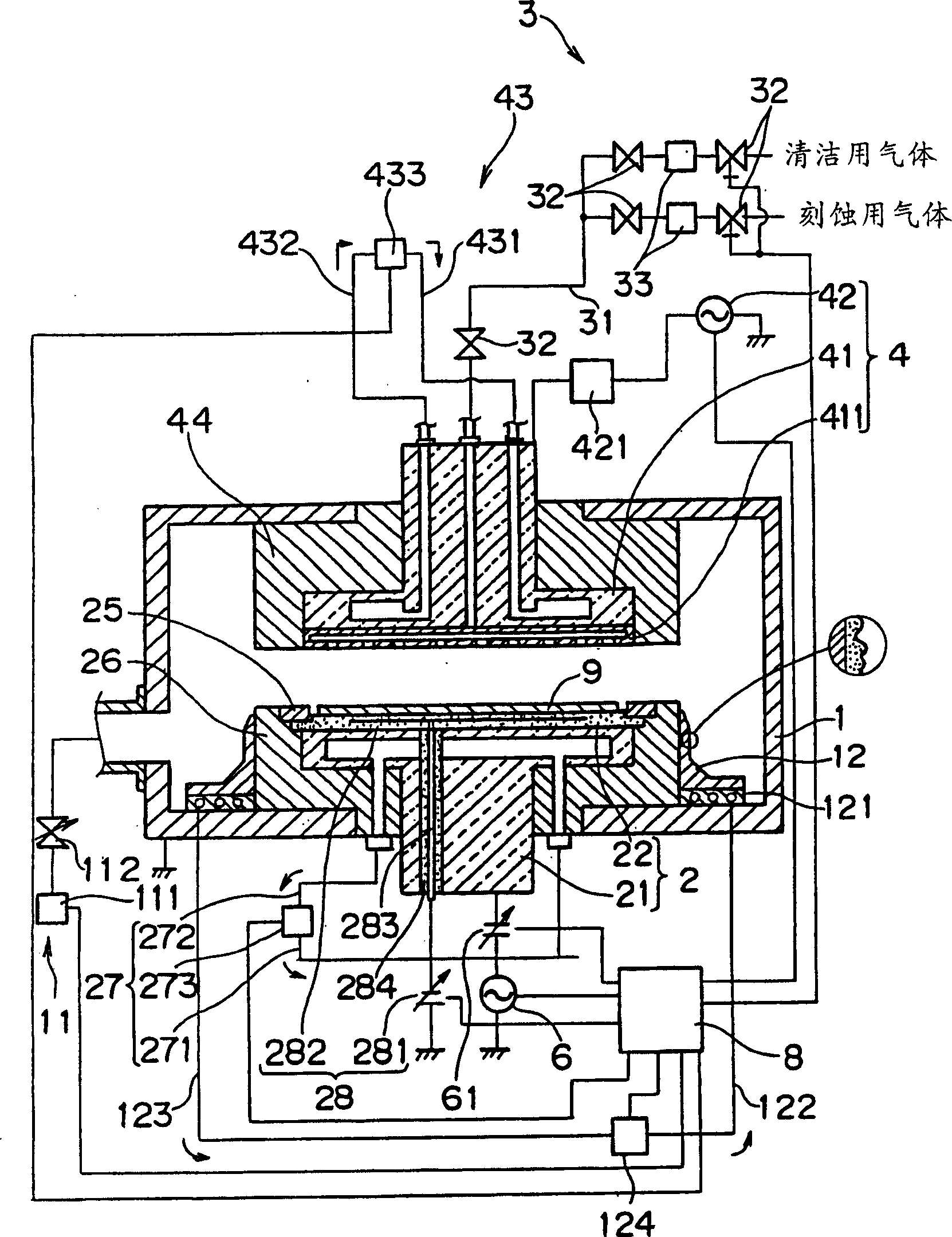
[0034] figure 1 is a schematic front cross-sectional view showing the structure of the main part of the insulating film etching apparatus according to the embodiment of the present invention. figure 1 The shown device has: a processing chamber 1, which has an exhaust system 11, and performs etching processing inside; a substrate holder 2, which keeps the substrate 9 at a predetermined position in the processing chamber 1; a gas introduction system 3, which controls the etching process. The gas is introduced into the processing chamber 1; the plasma forming device 4 forms the plasma of the introduced gas;

[0035] The processing chamber 1 is an airtight vacuum container. The processing chamber 1 is formed of metal such as stainless steel, and is electrically grounded. The exhaust system 11 is equipped with a vacuum pump 111 such as a dry pump and an exhaust speed regulator 112, and can maintain the inside of...


PUM


Abstract

This application discloses an insulation-film etching system that etches an insulator film on a substrate by a species produced in plasma. While the substrate (9) is held by a substrate holder (2) provided in a process chamber (1), an etching gas is introduced into the chamber (1) by a gas inlet system (3). An insulating film on the surface of the substrate (9) is etched by the action of an active species and ions contained in a plasma formed by a plasma forming means (4). After completion of the etching, a control section (8) takes out the substrate (9) from the process chamber (1) by a transport robot (51) and evacuates the chamber (1) by an exhaust system. Then the section (8) removes films deposited on exposed surfaces in the chamber (1) by the action of a plasma formed by the plasma forming means (4) by introducing a cleaning gas by the gas inlet system (3). A cooling trap (12) provided at a level lower than the substrate holding surface of the substrate holder (2) is forcibly cooled and causes many films to deposit by collecting gas molecules which tend to deposit. The trap (12) is replaceable and the surface of the trap (12) has irregularity sections to prevent the peeling of deposited films. The surfaces of the irregularity sections are composed of an oxide or insulator.

Description

technical field [0001] The invention relates to an insulating film etching device for etching an insulating film on the surface of a substrate. Background technique [0002] Surface treatment of substrates is popular in the manufacturing process of electronic devices such as LSI (Large Scale Integration) and LCD (Liquid Crystal Display). Among them, the process of etching the insulating film on the surface of the substrate is one of the main processes when forming fine circuits. For example, a resist pattern is formed by photolithography on a silicon substrate whose surface is covered with an insulating film such as a silicon oxide film or a silicon nitride film, and this is used as a mask to form the insulating film along the shape of the resist pattern. etch. In addition, fine wiring is formed by embedding tungsten, aluminum, or the like in the etched portion. [0003] As an insulating film etching device, dry etching using plasma is the mainstream. Specifically, gas i...

Claims


Application Information

Patent Timeline
Patent Type & Authority Applications(China)
IPC IPC(8): H01L21/302H01L21/00H01L21/3065
CPCH01L21/67028H01L21/67253H01L21/67069H01L21/3065
Inventor 佐护康实小河原米一宫前昌典
Owner ANELVA CORP
Why Eureka
Try Eureka