Level shift circuit

A technology of level shifting and circuit, which is applied in the direction of circuit, logic circuit connection/interface layout, electrical components, etc. It can solve the problems of slow action and deterioration of level shifting circuit action speed, and achieve the effect of suppressing hysteresis effect and action delay Discrete effect

Inactive Publication Date: 2003-07-30
SOCIONEXT INC
View PDF1 Cites 8 Cited by
  • Summary
  • Abstract
  • Description
  • Claims
  • Application Information

AI Technical Summary

Problems solved by technology

As a result, in the process of changing these signals IN and XIN from 0V to a specified voltage level (0.7V), the operation of the N-channel transistors 1 and 2 that switch to the conduction state is slow, resulting in a level shift circuit Overall movement speed deteriorates

Method used


Image

  • Level shift circuit
  • Level shift circuit
  • Level shift circuit

Examples


no. 1 Embodiment

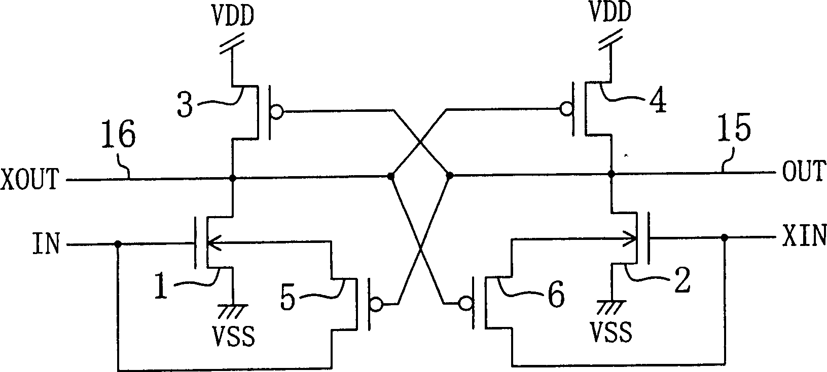
[0050] figure 1 A level shift circuit according to a first embodiment of the present invention is shown. In this figure, VDD is a high-voltage power supply, VSS is a ground power supply, IN is an input signal, XIN is an inverted input signal, OUT is an output signal, and XOUT is an inverted output signal.

[0051] In addition, 1 is a first N-channel transistor for signal input to which the input signal IN is input to the gate, and 2 is a first N-channel transistor for signal input to which the inverted input signal XIN is input to the gate. 2N-channel transistors, the sources of the two transistors 1 and 2 are connected to the ground voltage VSS. 3 and 4 are the first and second P-channel transistors whose sources are connected to the high-voltage power supply VDD, and between these two P-channel transistors 3 and 4, a gate of a P-channel transistor is formed. pole is connected to the cross-coupling connection of the drain of another P-channel type transistor. The drain of...

no. 2 Embodiment

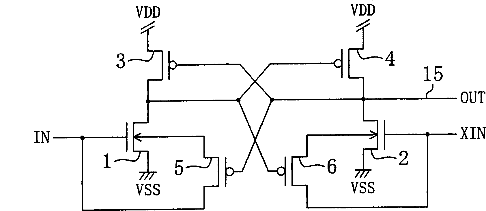
[0070] Figure 7 A level shift circuit according to a second embodiment of the present invention is shown.

[0071] The level shift circuit shown in this figure has the following features: First and second N-channel transistors 7 and 8 for resetting are added to the structure of the level shift circuit of the first embodiment described above. The source of the first N-channel transistor 7 used for reset is connected to the ground power supply (low power supply voltage) VSS, the drain is connected to the substrate of the first N-channel transistor 1 for signal input, and the The output signal OUT of the signal line 15 is input to the gate. Similarly, the source of the 2nd N-channel transistor 8 for reset is connected to the ground power supply (low power supply voltage) VSS, and the drain is connected to the substrate of the 2nd N-channel transistor 2 for signal input. , the inverted output signal XOUT of the signal line 16 is input to the gate.

[0072] In this embodiment, ...

no. 3 Embodiment

[0078] Figure 9 A level shift circuit according to a third embodiment of the present invention is shown. The level shifting circuit of this figure has the following features: In the above Figure 7 In the configuration of the level shift circuit of the second embodiment shown, first and second delay elements 9 and 10 are added. The first delay element 9 is arranged between the signal line 15 for outputting the signal OUT and the gate of the first N-channel transistor 7 for reset. The second delay element 10 is arranged between the signal line 16 of the inverted output signal XOUT and the gate of the second N-channel transistor 8 for reset.

[0079] The level shifting circuit of this embodiment has the structure of the level shifting circuit of the above-mentioned second embodiment, so as described above, only when the input signal IN and the inverted input signal XIN rise and change, these signals are received on the gate The N-channel transistors 1 and 2 have a substrate ...


PUM


Abstract

In a level shift circuit according to the invention, either an input signal IN or an inverted input signal XIN, which are input into the gate electrodes of n-type transistors 1, 2 for signal input, is also given to the substrate of that n-type transistor via p-type transistors 5, 6 for substrate bias. When the signal IN or XIN rises and changes, the threshold voltages of the n-type transistors 1, 2 for signal input is lowered due to the substrate bias effect. Consequently, even if the signal IN or XIN has a low voltage level, operation is carried out at high speeds. Also, when either an output signal OUT or an inverted output signal XOUT is changed to a high voltage level, the transistors 5, 6 for substrate bias become non-conducting, and thus the input signal IN or the inverted input signal XIN is not supplied to the substrate of the n-type transistors 1, 2 for signal input other than when the signal is changing. Consequently, a constant passing-through current does not flow to the substrate of these transistors.

Description

technical field [0001] The present invention relates to level shifting circuits for interfacing between circuits having different supply voltages. Background technique [0002] With recent refinement of manufacturing, the power supply voltage of the internal circuits of semiconductor integrated circuits tends to be lowered due to the reliability of components. On the other hand, among the components used in systems such as electronic equipment, there are some components that continue to use the conventional power supply voltage. In order to achieve connection between these elements having different power supply voltages and the semiconductor integrated circuit, a level shift circuit is generally built in the semiconductor integrated circuit. [0003] Recently, even in semiconductor integrated circuits, in order to reduce power consumption, measures have been taken to supply optimal power supply voltages to each circuit block, and in order to obtain the connection between th...

Claims


Application Information

Patent Timeline
Patent Type & Authority Applications(China)
IPC IPC(8): H03K19/0185H03K3/012H03K3/356
CPCH03K3/356113H03K3/012
Inventor 祗园雅弘
Owner SOCIONEXT INC
Why Eureka
Try Eureka