Method of improving performance of flash memory

A memory, flash technology, applied in semiconductor/solid-state device manufacturing, electrical components, circuits, etc., can solve the problems of oxygen-nitrogen-oxygen layer erosion, performance degradation of flash memory, etc.

Inactive Publication Date: 2003-08-20
MACRONIX INT CO LTD
View PDF0 Cites 0 Cited by
  • Summary
  • Abstract
  • Description
  • Claims
  • Application Information

AI Technical Summary

Problems solved by technology

[0010] In the prior art of unit cell oxidation, no matter using dry oxidation method, wet oxidation method or dry rapid oxidation method, serious oxygen-nitrogen-oxygen layer erosion phenomenon will occur, thus causing the oxygen-nitrogen-oxygen layer to be damaged. The increase in the thickness of the double oxide layer will inevitably increase the operating voltage, resulting in a decrease in the performance of the flash memory

Method used


Image

  • Method of improving performance of flash memory
  • Method of improving performance of flash memory
  • Method of improving performance of flash memory

Examples


Embodiment Construction

[0029] Such as Figure 5Shown is a cross-sectional view of a typical flash memory unit cell, the memory unit usually includes a substrate 100 and a thin gate oxide layer 110 (usually as a tunnel oxide layer) formed on the surface of the substrate 100, two The stacked gate structure 160 is located on the gate oxide layer 110 . The stacked gate structure 160 also includes a first polysilicon layer as a floating gate 120 on the tunnel oxide layer 110, an inner poly dielectric layer 130 on the floating gate 120, and finally, a second polysilicon layer layer overlies the inner poly dielectric layer 130 as a control gate 140 .

[0030] Such as Figure 5 As shown, the stacked gate structure 160 is formed using conventional etching methods. However, a problem usually created by this step is the formation of polysilicon residue 150 . The polysilicon residue 150 is formed by etching the unmasked part of the polysilicon layer 120. The material of the polysilicon residue 150 is mainly...


PUM


Abstract

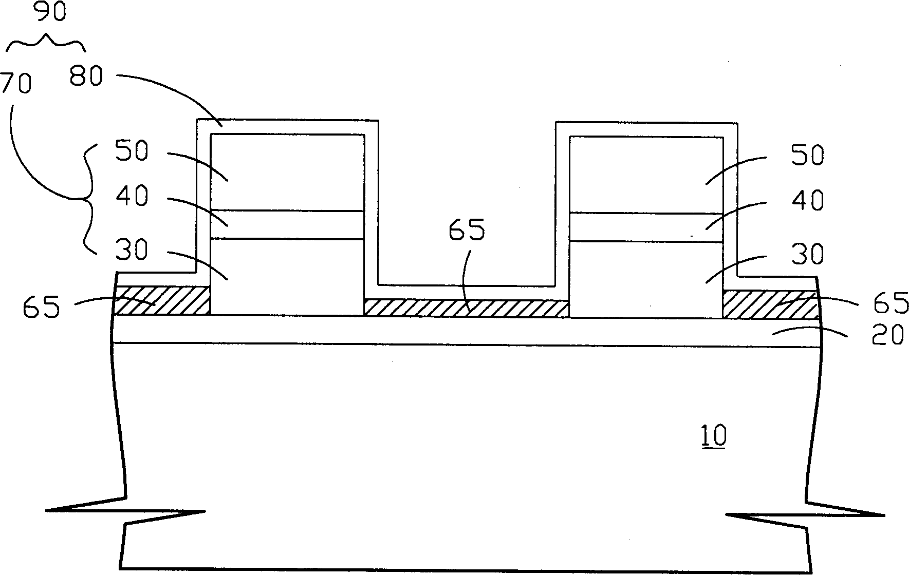
The method of improving performance of flash memory includes providing one substrate; forming one tunneling oxide layer on the substrate; forming on the tunneling oxide layer two grid structures, each of which includes the first polysilicon layer as floating grid, one inner polycrystal dielectric layer, such as O-N-O layer on the floating grid and the second polysilicon layer as control grid on the inner polycrystal dielectric layer, and oxidizing crystal cell with oxygen free radical with slight erosion on the O-N-O layer, about 6% increase of grid capacitance coupling ratio, increase of 5 times in operation speed and elimination of residual polysilicon.

Description

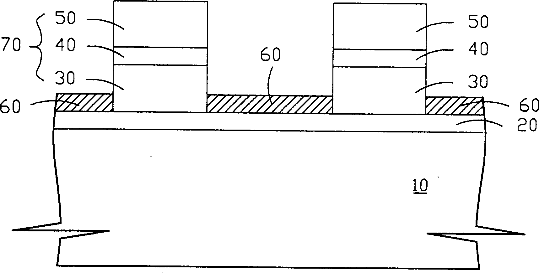
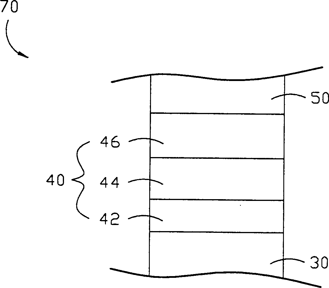
(1) Technical field [0001] The present invention relates to a method for manufacturing flash memory, and more particularly to a method for promoting the performance of flash memory by utilizing the O radical cell oxidation step. (2) Background technology [0002] The non-volatile memory element includes a flash erasable programmable read only memory (EEPROM, electrical erasable programmable read only memory). figure 1 Shown is a cross-sectional view of a typical flash memory unit cell. The memory cell usually includes a substrate 10 and a thin gate oxide 20 (usually used as a tunnel oxide )) is formed on the surface of the substrate 10 , and two stacked gate structures 70 are located on the gate oxide layer 20 . The stacked gate structure 70 includes a first polysilicon layer as a floating gate 30 on the tunnel oxide layer 20 , and an interpoly dielectric layer 40 on the floating gate 30 , and finally, the second polysilicon layer overlaps the inner polysilicon dielectric ...

Claims


Application Information

Patent Timeline
Patent Type & Authority Applications(China)
IPC IPC(8): H01L21/82H01L21/8239
Inventor 韩宗廷苏俊联苏金达
Owner MACRONIX INT CO LTD
Why Eureka
Try Eureka