Structure of flash memory cell and method for making the same

A technology of storage unit and manufacturing method, applied in semiconductor/solid-state device manufacturing, electrical components, electric solid-state devices, etc.

Inactive Publication Date: 2003-10-15
WINBOND ELECTRONICS CORP
View PDF0 Cites 3 Cited by
  • Summary
  • Abstract
  • Description
  • Claims
  • Application Information

AI Technical Summary

Problems solved by technology

On the other hand, when manufacturing flash memory cells using common methods, it is impossible to effectively increase the coupling

Method used


Image

  • Structure of flash memory cell and method for making the same
  • Structure of flash memory cell and method for making the same
  • Structure of flash memory cell and method for making the same

Examples


Embodiment Construction

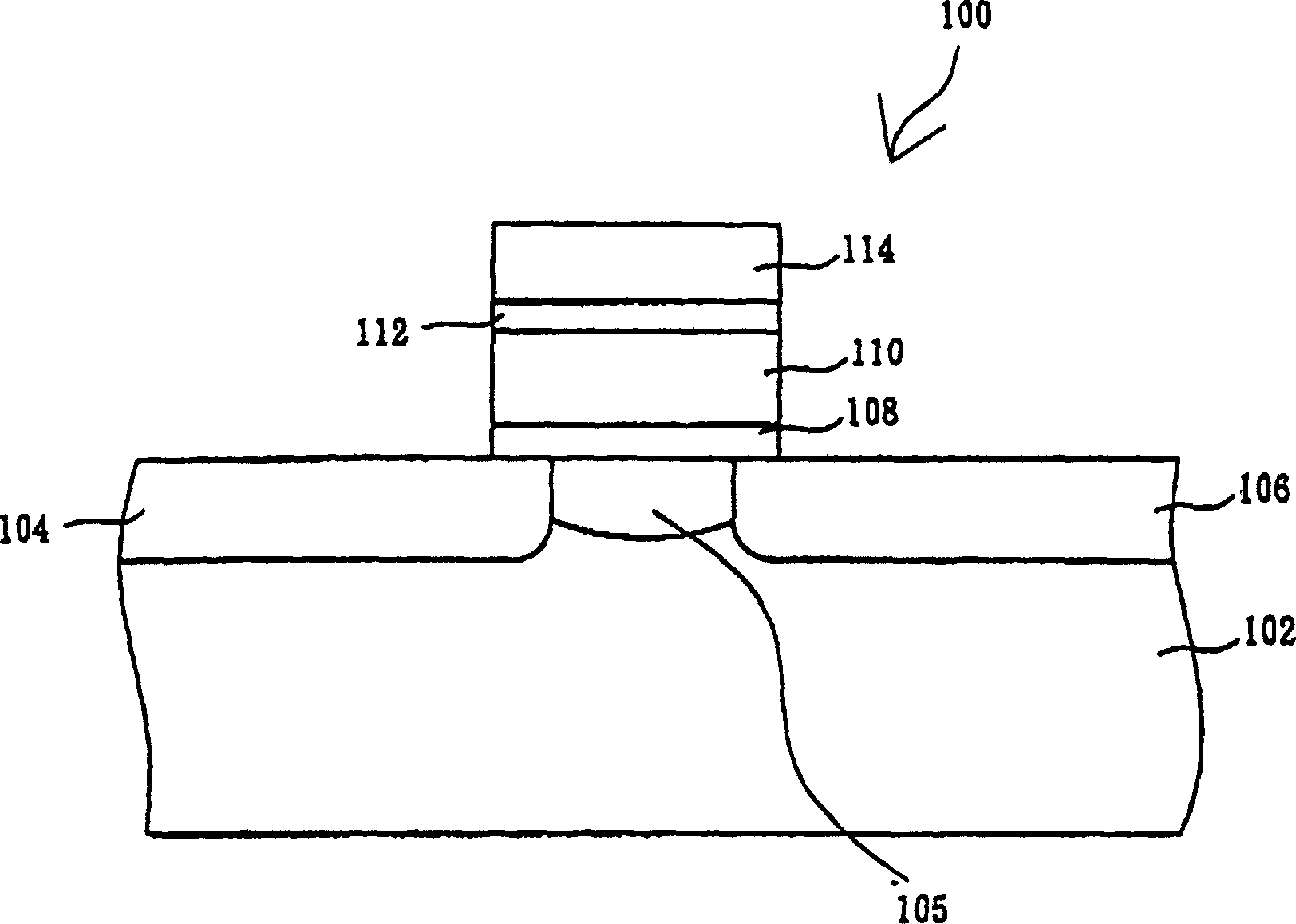
[0032] The invention discloses a structure of a flash storage unit and a manufacturing method thereof. The flash memory unit of the present invention has a planar surrounding gate, and can use FN tunneling effect to write and erase data. In addition to effectively improving the leakage current between the source and the drain and increasing the cell current in the on state, it can also achieve the purpose of improving the performance of the device without increasing the size of the device. In order to make the narration of the present invention more detailed and complete, refer to the following description and cooperate Figure 2 to Figure 15 .

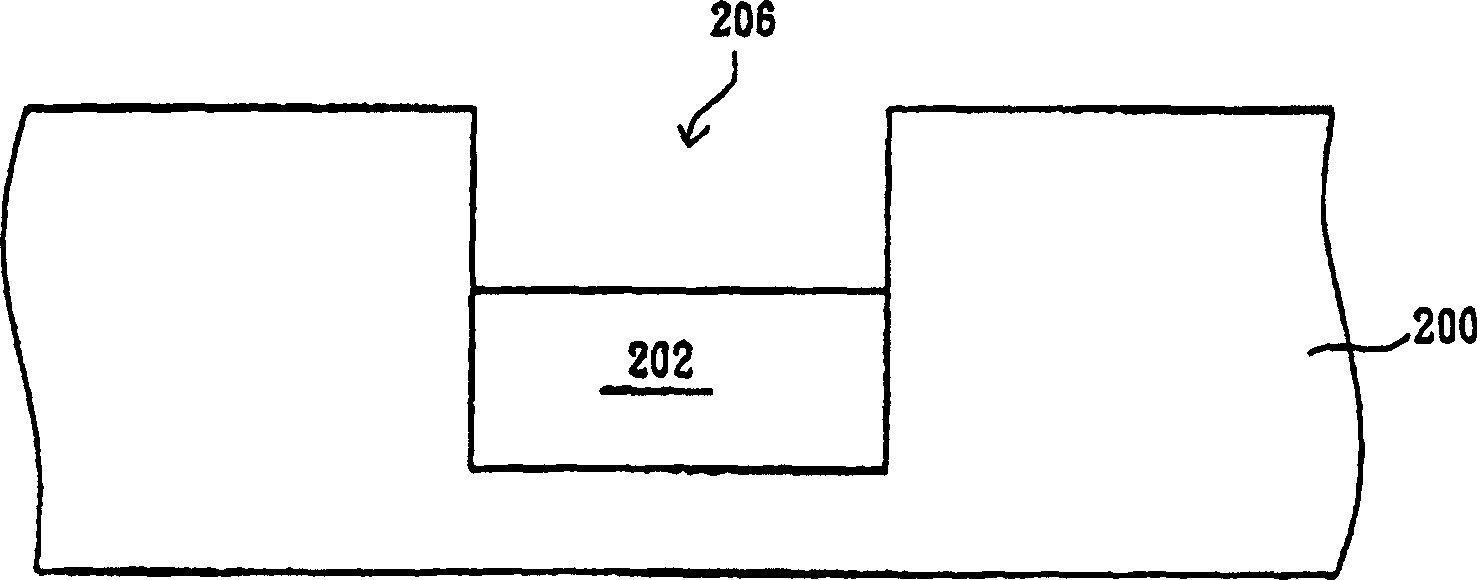
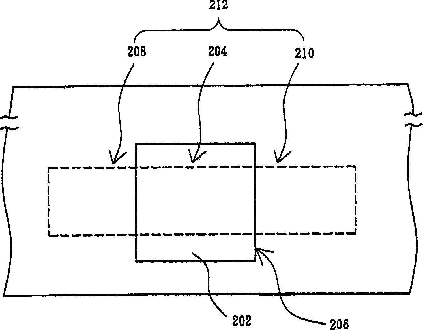
[0033] Please refer to figure 2 and Tutu, where image 3 for figure 2 top view. First, a plurality of isolation regions 202 are formed on the semiconductor substrate 200 (only the isolation regions 202 located in the preset device region 212 are shown), part of the isolation regions 202 are used to isolate devices, and the othe...


PUM


Abstract

The present invention relates to the structure and manufacture of flash memory cell with horizontal surrounding gate. The flash memory cell is formed inside the channel of isolating area, and its signal channel is formed with semiconductor film and is coated and surrounded by tunneling oxide layer, floating gate, dielectric layer and control gate successively. The floating gate and the control gate are also formed inside the channel below the signal channel. Therefore, there are less signal channel leakage current, no short signal channel effect, and raised coupling capacitance between the floating gate and the control gate. In addition, during data programming and erasing, Fowler-Nordheim tunneling process may be adopted.

Description

technical field [0001] The present invention relates to a structure of a flash memory cell (Flash Memory Cell) and a manufacturing method thereof, in particular to a flash memory cell with source (Source) / drain (Drain) writing (Programming) and erasing (Erasing) The structure of the flash memory unit and its manufacturing method. Background technique [0002] With the continuous improvement of semiconductor manufacturing technology, the vigorous development of computer, communication, network industry, and information appliance (IA) has been brought about. Because reducing the size of the device can not only improve the integration of the circuit device and reduce the cost, but also improve the switching speed of the device and the power consumption of the device, and strengthen its information storage, logic operation, signal processing and other functions. Therefore, reducing the size of semiconductor devices has become the main driving force for promoting the progress of...

Claims


Application Information

Patent Timeline
IPC IPC(8): H01L21/8246H01L27/112
Inventor 张文岳
Owner WINBOND ELECTRONICS CORP
Why Eureka
Try Eureka