Structure of flash memory unit with planar surround grid and its manufacturing methods

A technology of storage unit and manufacturing method, which is applied in semiconductor/solid-state device manufacturing, electrical components, electric solid-state devices, etc., and can solve problems such as leakage current deterioration and leakage current deterioration

Inactive Publication Date: 2005-11-23
WINBOND ELECTRONICS CORP
View PDF0 Cites 0 Cited by
  • Summary
  • Abstract
  • Description
  • Claims
  • Application Information

AI Technical Summary

Problems solved by technology

Therefore, the situation of leakage current will be worsened
[0010] In the above-mentioned common flash memory cell structure, the leakage current phenomenon between the source and the drain is getting worse
Moreover, it is impossible to effectively increase the coupling capacitance between the control gate and the floating gate without increasing the cell size and the cost of the fabrication method.

Method used


Image

  • Structure of flash memory unit with planar surround grid and its manufacturing methods
  • Structure of flash memory unit with planar surround grid and its manufacturing methods
  • Structure of flash memory unit with planar surround grid and its manufacturing methods

Examples


Embodiment Construction

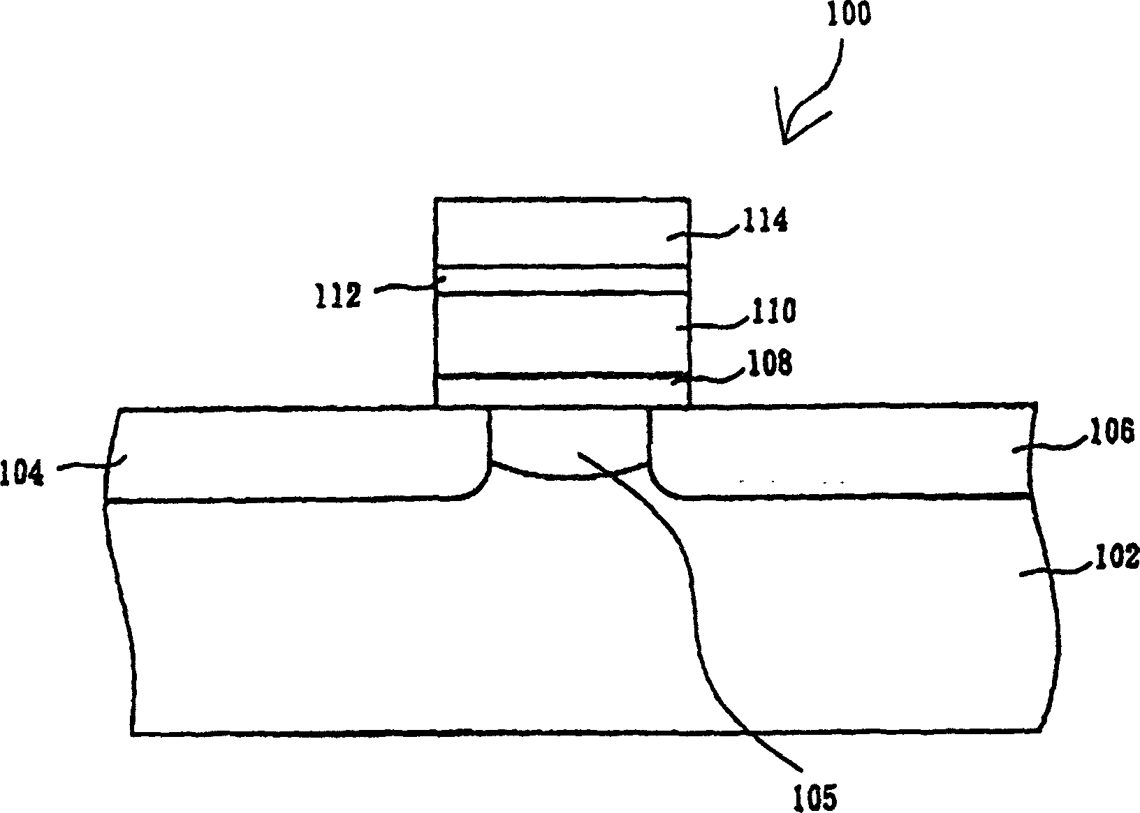
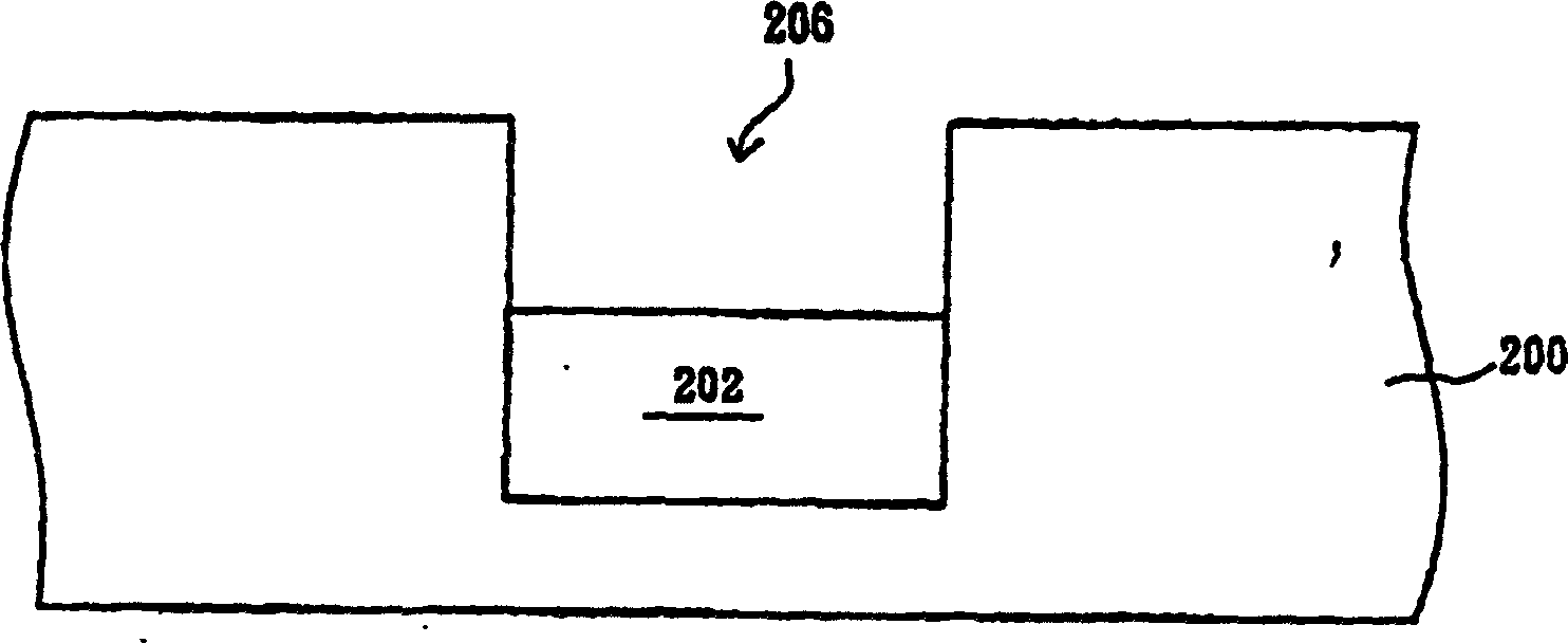
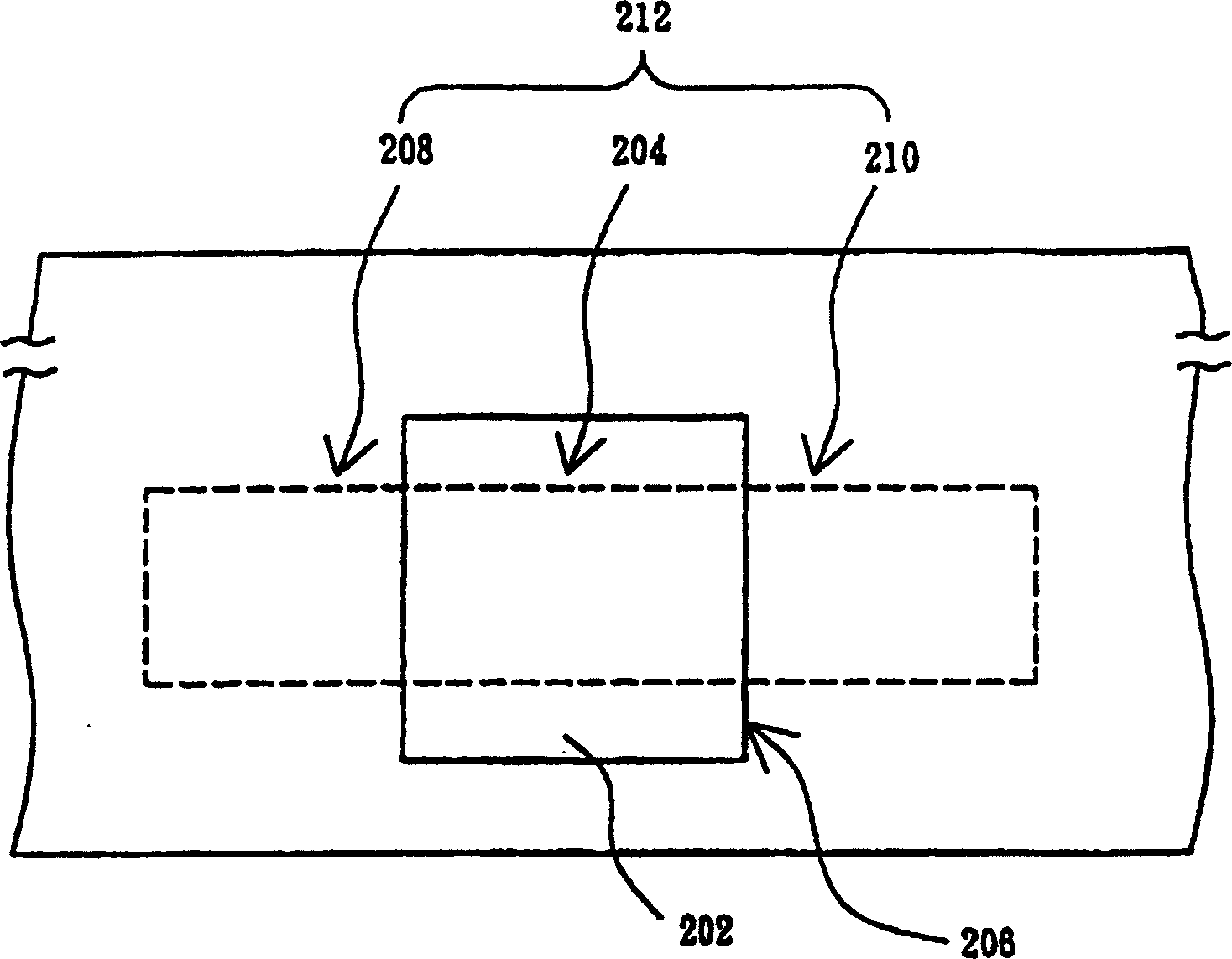
[0029] With the popularization of portable electronic products, the demand for flash memory is greatly increased. How to develop a new generation of flash memory and reduce the size of flash memory cells has become an important research trend. The invention discloses a structure of a planar surrounding gate flash memory unit and a manufacturing method thereof. The planar surrounding gate flash memory unit of the invention can effectively reduce the leakage current between the source and the drain, and can increase the unit current in the open state. Moreover, a higher capacitive coupling ratio between the floating gate and the control gate can be obtained without changing the unit size, so as to achieve the purpose of reducing the writing / erasing voltage of the flash memory unit. In order to make the narration of the present invention more detailed and complete, refer to the following description and cooperate Figure 2 to Figure 15 icon. Please refer to figure 2 as well ...


PUM


Abstract

A flash memory cell is located in the channel in insulation region. The channel region is composed of the semiconductor films, which surrounds the channel in sequence: the tunneling oxide layer, the floating gate and the control gate. The floating gate and the control gate are formed on the groove under channel region at same time so as to improve the state of the leakage current. The depth of junction of the source and drain does not caused the short channel effect. Moreover, increasing depth of the channel can raise the coupling capacitor between the control gate and the floating gate easily.

Description

technical field [0001] The present invention relates to a flash memory (Flash Memory) and a manufacturing method thereof, in particular to a structure of a planar horizontal surrounding gate (Horizontal Surrounding Gate; HSG) flash memory unit (Cell) and a manufacturing method thereof. Background technique [0002] The continuous innovation of semiconductor manufacturing technology has brought about the vigorous development of computers, communications, network industries, and data appliances (IA). The main driving force behind the progress of semiconductor manufacturing technology is to reduce the size of semiconductor devices. Reduce the size of the device to improve the switching speed and power consumption of the device, increase the integration of the circuit device, and strengthen its data storage, logic operation, signal processing and other functions, and reduce the cost. In particular, the semiconductor memory device, which occupies a very important position in the...

Claims


Application Information

Patent Timeline
Patent Type & Authority Patents(China)
IPC IPC(8): H01L21/8246H01L27/112
Inventor 张文岳
Owner WINBOND ELECTRONICS CORP
Why Eureka
Try Eureka