

Flash memory and method of forming the same
A memory and flash technology, applied in the field of flash memory and its formation, can solve the problems affecting the performance of flash memory, small capacitive coupling rate, and reduced facing area, so as to improve operation speed and efficiency, and improve capacitive coupling. rate, improve performance
- Summary
- Abstract
- Description
- Claims
- Application Information
AI Technical Summary
Problems solved by technology
Method used
Image

Examples
no. 1 example
[0043] This embodiment provides a method for forming a flash memory, including:
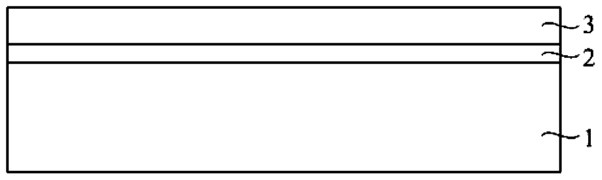
[0044] refer to Figure 5 , providing a substrate 110 on which a first dielectric material layer 120 is formed.
[0045] In a specific embodiment, the method of forming the first dielectric material layer 120 is chemical vapor deposition, physical vapor deposition or atomic layer deposition.
[0046] In a specific embodiment, the material of the first dielectric material layer 120 is a low-k material, such as one or more of amorphous carbon nitrogen, polycrystalline boron nitrogen, fluorosilicate glass, porous SiOCH and porous diamond. The upper surface of the substrate 110 may also be oxidized by a thermal oxidation method, and the formed oxide layer serves as the first dielectric material layer 120 .
[0047] In a specific embodiment, before forming the first dielectric material layer 120 , it further includes forming a source S and a drain D (not shown) in the substrate 110 .
[0048] The m...
no. 2 example
[0078] The difference between this embodiment and the first embodiment is:
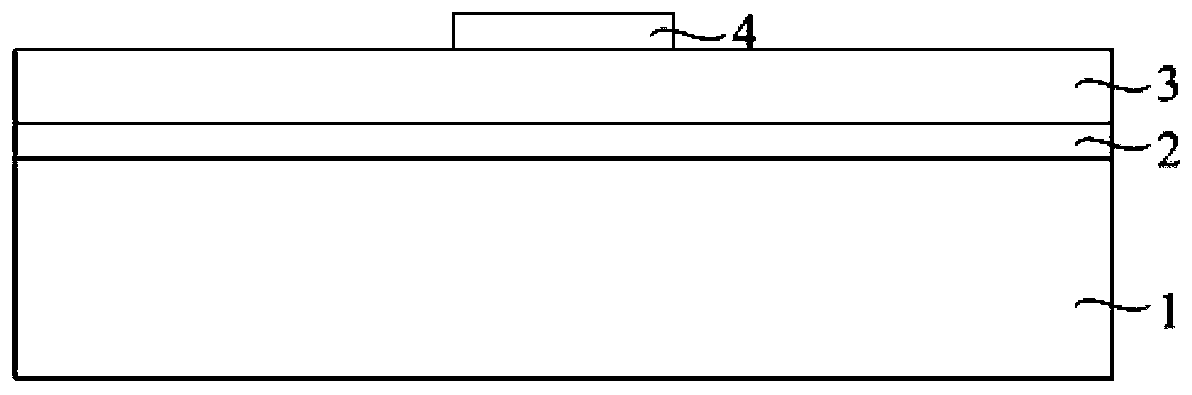
[0079] refer to Figure 13 After depositing the floating gate material layer 130 on the tunnel dielectric layer 123, a patterned mask layer 104 is formed on the floating gate material layer 130, and the patterned mask layer 104 defines location of the floating gate.
[0080] Since the floating gate is to cover the upper surface and the sidewall of the protrusion 102, the patterned mask layer 104 must be located directly above the protrusion 102, and the patterned mask layer The width of 104 should be greater than the width of the protrusion 102 .
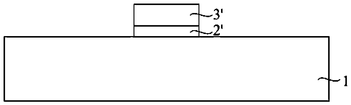
[0081] refer to Figure 14 , using the patterned mask layer 104 as a mask to etch the floating gate material layer 130 up to the upper surface of the tunnel dielectric layer 123 to form the floating gate 131 . After the floating gate 131 is formed, the patterned mask layer 104 is removed.
[0082] refer to Figure 15 , forming an inter-gate dielectric...
no. 3 example
[0091] The difference between the third embodiment and the first embodiment lies in that the method for forming the tunnel dielectric layer is different.
[0092] In the third embodiment, the method for forming the tunnel dielectric layer is:
[0093] refer to Figure 16 , forming a first dielectric material layer 120 on the substrate 110; forming a patterned mask layer 101 on the first dielectric material layer 120, and the patterned mask layer 101 defines the positions of the protrusions.
[0094] In a specific embodiment, the thickness of the first dielectric material layer 120 in this embodiment is equal to the sum of the thicknesses of the first dielectric material layer 120 and the second dielectric material layer 122 in the first embodiment.
[0095] For this step, reference may be made to the relevant steps in the first embodiment.
[0096] refer to Figure 17 , using the patterned mask layer 101 as a mask to etch a partial thickness of the first dielectric material...
PUM
 Abstract
Description
Claims
Application Information