Strong dielectric memory
A ferroelectric and storage device technology, applied in information storage, static memory, digital memory information, etc., can solve the problems of large memory area and inability to increase capacity, and achieve the effect of reducing power consumption
- Summary
- Abstract
- Description
- Claims
- Application Information
AI Technical Summary
Problems solved by technology
Method used
Image
Examples
no. 1 Embodiment approach
[0034] (Explanation of its structure)
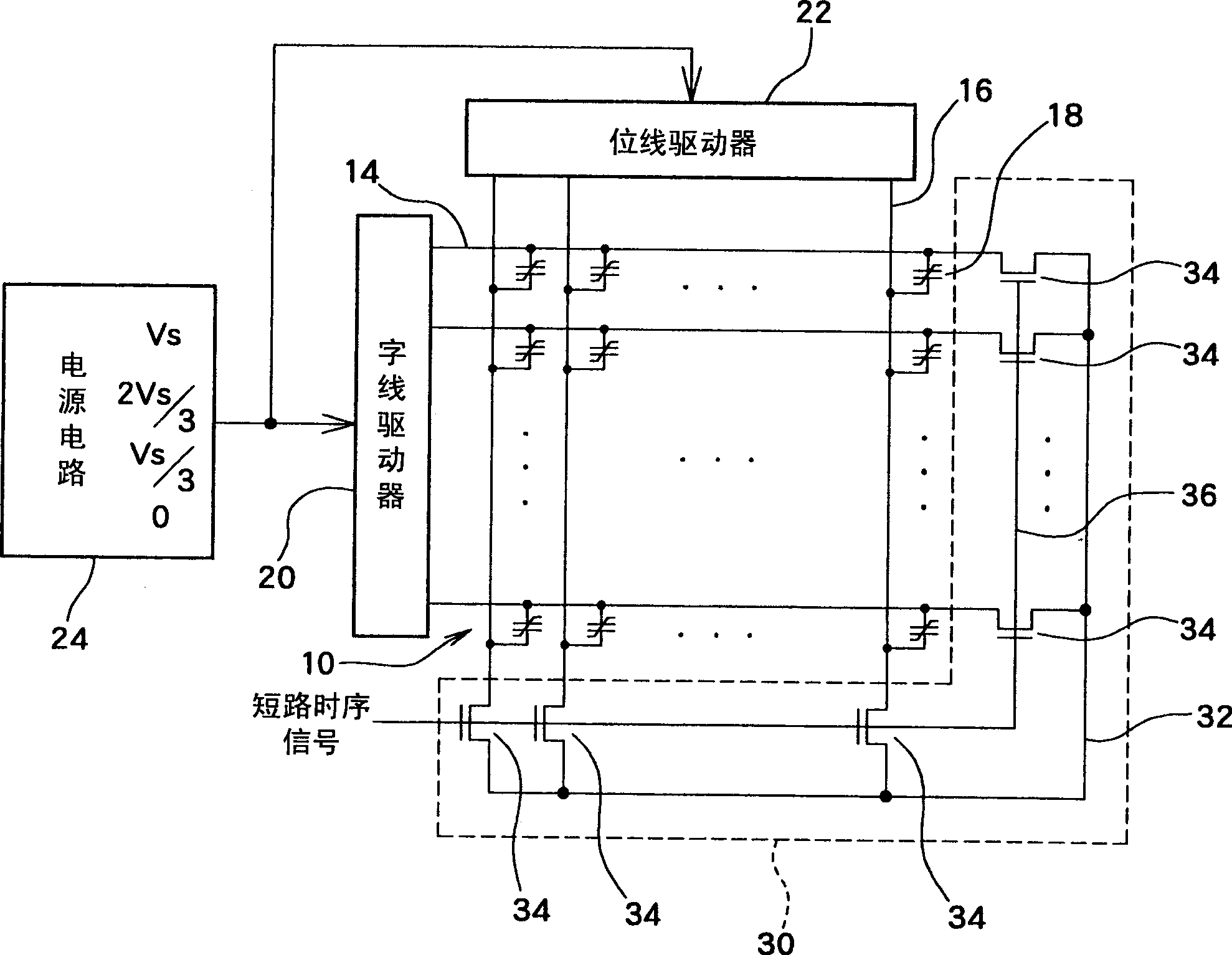
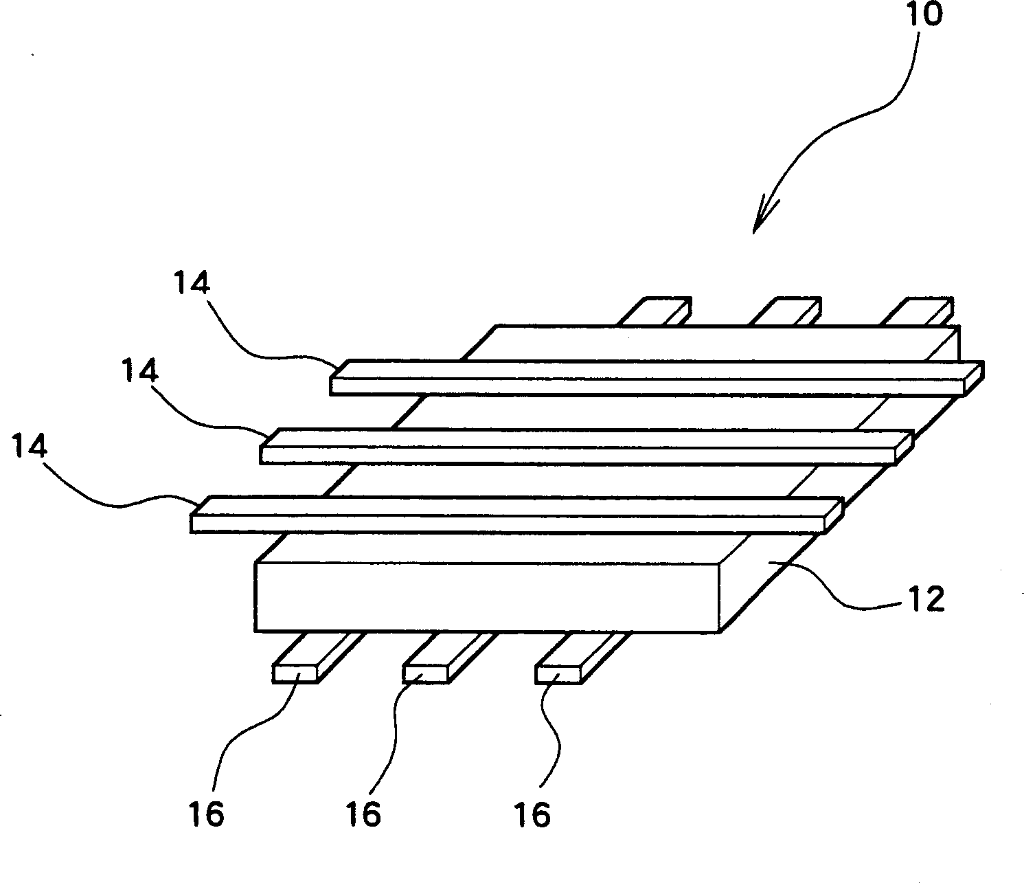
[0035] figure 1 It is a block diagram of FeRAM of the ferroelectric memory device related to the first embodiment of the present invention, figure 2 A three-dimensional view of its storage array for the model. Such as figure 2 As shown, the memory cell array 10 has a ferroelectric film 12 , a plurality of word lines 14 arranged on one side of the ferroelectric film 12 , and a plurality of bit lines 16 arranged on the other side of the ferroelectric film 12 .
[0036] With the above structure, at each intersection (intersection type) of the plurality of word lines 14 and the plurality of bit lines 16, as figure 1 As shown, the ferroelectric memory cells 18 are respectively formed. According to this construction, as figure 2 The memory shown is called a cross-point type FeRAM or a passive type FeRAM. In this way, if figure 2 The shown memory is different from an active memory having a 1T / 1C cell in which a transistor and a capac...
no. 4 Embodiment approach
[0087] Figure 13 expresses the replacement Figure 10 The power-on timing generating circuit 40 shown is the fourth embodiment of the present invention provided with a power-on timing generating circuit 42 .
[0088] Separately Figure 13 An example of the power-on timing generation circuit 42 shown is shown in Figure 14 , express its action sequence diagram in Figure 15 middle. The output PEQ2 of the power-off sequence generation circuit 42, such as Figure 15 When disconnected from the power supply voltage Vcc as shown (at Figure 15 The falling edge time t0) of the middle power supply off signal rises synchronously, and even after the power supply voltage Vcc becomes 0V, after a predetermined period of time, it can reach above the threshold voltage Vth of the N-type MOS transistor 34 of the short-circuit switch 34 constituting the short-circuit circuit 30. . In this way, the short-circuit operation in the short-circuit circuit 30 can be performed even when the pow...
no. 5 Embodiment approach
[0091] Figure 16 for settings such as Figure 10 shown in the power-on timing generation circuit 40 and Figure 13 A block diagram of a fifth embodiment of the present invention of a power-on timing generating circuit 42 is shown. exist Figure 16 In, there are a plurality of first short-circuit switches (NMOS) 34A connected between each end of the word line 14 and bit line 16 and the common short-circuit line 32, and a power-on switch is connected to the common gate control line 36A. Timing generation circuit 40. Furthermore, a plurality of second short-circuit switches 34B are provided in parallel with each of the plurality of first short-circuit switches, and the power-off timing generating circuit 42 is connected to the common gate line 36B. In this way, when the power is turned on, the plurality of first short-circuit switches 34A can be turned on, and when the power is turned off, the plurality of second short-circuit switches 34B can be turned on. In this way, the...
PUM
 Abstract
Description
Claims
Application Information


