Field effect transistor adapted for extra-dup submicrometer field and preparation process thereof

A field-effect transistor, ultra-deep sub-micron technology, applied in semiconductor/solid-state device manufacturing, semiconductor devices, electrical components, etc., to achieve the effects of ensuring overdrive capability, suppressing inter-band tunneling current, and reducing source-drain parasitic capacitance

Inactive Publication Date: 2003-10-22
SEMICON MFG INT (SHANGHAI) CORP +1
View PDF0 Cites 12 Cited by
  • Summary
  • Abstract
  • Description
  • Claims
  • Application Information

AI Technical Summary

Problems solved by technology

[0008] None of the above methods can achieve a good trade-off be

Method used


Image

  • Field effect transistor adapted for extra-dup submicrometer field and preparation process thereof
  • Field effect transistor adapted for extra-dup submicrometer field and preparation process thereof
  • Field effect transistor adapted for extra-dup submicrometer field and preparation process thereof

Examples


Embodiment Construction

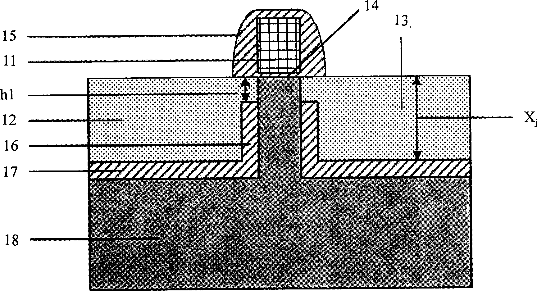
[0056] As shown in FIG. 1( a ), it is a schematic diagram of the field effect transistor structure of the present invention. In this field effect transistor structure, the most important components are the first dielectric isolation layer and the second dielectric isolation layer. The first dielectric isolation layer is between the source and drain and the body region, and is perpendicular to the direction of the channel. The second dielectric isolation layer is located under the source and drain and parallel to the direction of the channel. The two are connected into an "L" shape. There is a certain distance between "L" and the surface of the silicon chip, which is the connection between the source and drain and the channel. The first dielectric isolation layer of the vertical part is formed of silicon nitride, and the second dielectric isolation layer of the horizontal part is formed of a void layer.

[0057] The above-mentioned field effect transistor is manufactured usi...


PUM


Abstract

A fieldistor includes a source-drain, grating medium, grating electrode, channel and a substrate in which, a first medium isolation layer is vortical to the channel direction between the source-drainand the substrate, a connection part of the source-drain and the channel is between top of the first medium isolation layer and the channel surface, a second medium isolation layer parallel to the channel and between the source-drain bottom and substrate is formed to a L shape with the first. Optional extending technology is applied to prepare the first medium layer then to inject combined HHe toprepare the second medium isolation layer, controlling short channel effect.

Description

technical field [0001] The invention belongs to the technical field of the structure of a field effect transistor (Metal-Oxide-Silicon Field Effect Transistor) in a CMOS ultra-large-scale integrated circuit (ULSI) and its manufacturing method, especially the field effect transistor structure and its method of manufacture. Background technique [0002] With the CMOS VLSI technology entering the sub-0.1 micron field, the field effect transistors in the circuit have serious short channel effects, which is manifested by the decrease of the threshold voltage (threshold voltage) as the channel length decreases. The threshold voltage decreases as the drain terminal voltage increases, and the source-drain direct punch-through or off-state drain leakage current increases. The short channel effect will cause the field effect transistor to completely or partially fail to work, thereby causing circuit failure. Therefore, controlling the short channel effect is the most important subje...

Claims


Application Information

Patent Timeline
IPC IPC(8): H01L21/335H01L29/772
Inventor 黎明黄如杨胜齐张兴王阳元
Owner SEMICON MFG INT (SHANGHAI) CORP
Why Eureka
Try Eureka