Structure of LED electrode and producing method

A manufacturing method and electrode technology, applied to circuits, electrical components, semiconductor devices, etc., can solve problems such as reduced lifespan, damaged junctions, and opacity

Inactive Publication Date: 2003-11-26
张修恒
View PDF0 Cites 19 Cited by
  • Summary
  • Abstract
  • Description
  • Claims
  • Application Information

AI Technical Summary

Problems solved by technology

[0005] The known electrode is in the center so that the electric field can be evenly distributed to the surroundings, but gold and aluminum are opaque. If the electrode is too large, the light will be blocked a lot, and the light generated cannot be fully utilized. If the electrode is too small, the electric field will be excessively concentrated and the current will be reduced. Density increases and lifespan decreases; and a dark hole is formed in the middle, especially at close range
And this kind of elec

Method used


Image

  • Structure of LED electrode and producing method
  • Structure of LED electrode and producing method
  • Structure of LED electrode and producing method

Examples


Embodiment Construction

[0031] The content of the present invention can be disclosed through the following embodiments in conjunction with the relevant drawings. The color and material of the LED used in the present invention and the structure of the light-emitting diode are not limited, as long as the light-emitting diode that can emit light is applicable. The electrode structure of the present invention is suitable for lamination packaging of light-emitting diodes of different colors, so as to obtain light of another color or white light by mixing light of two colors or three colors.

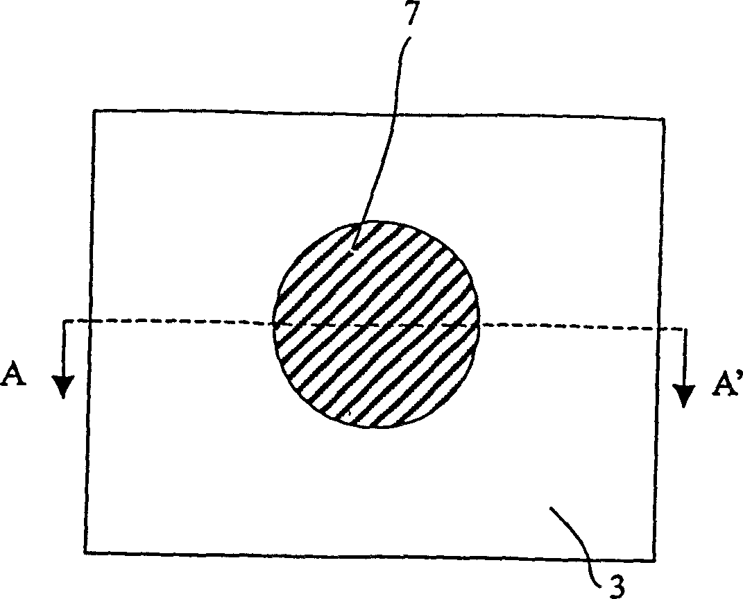
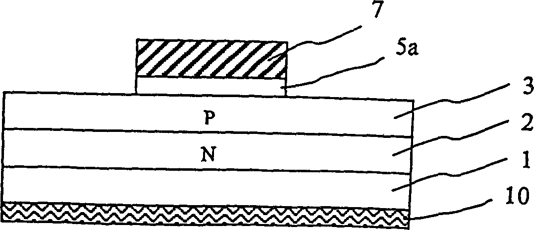
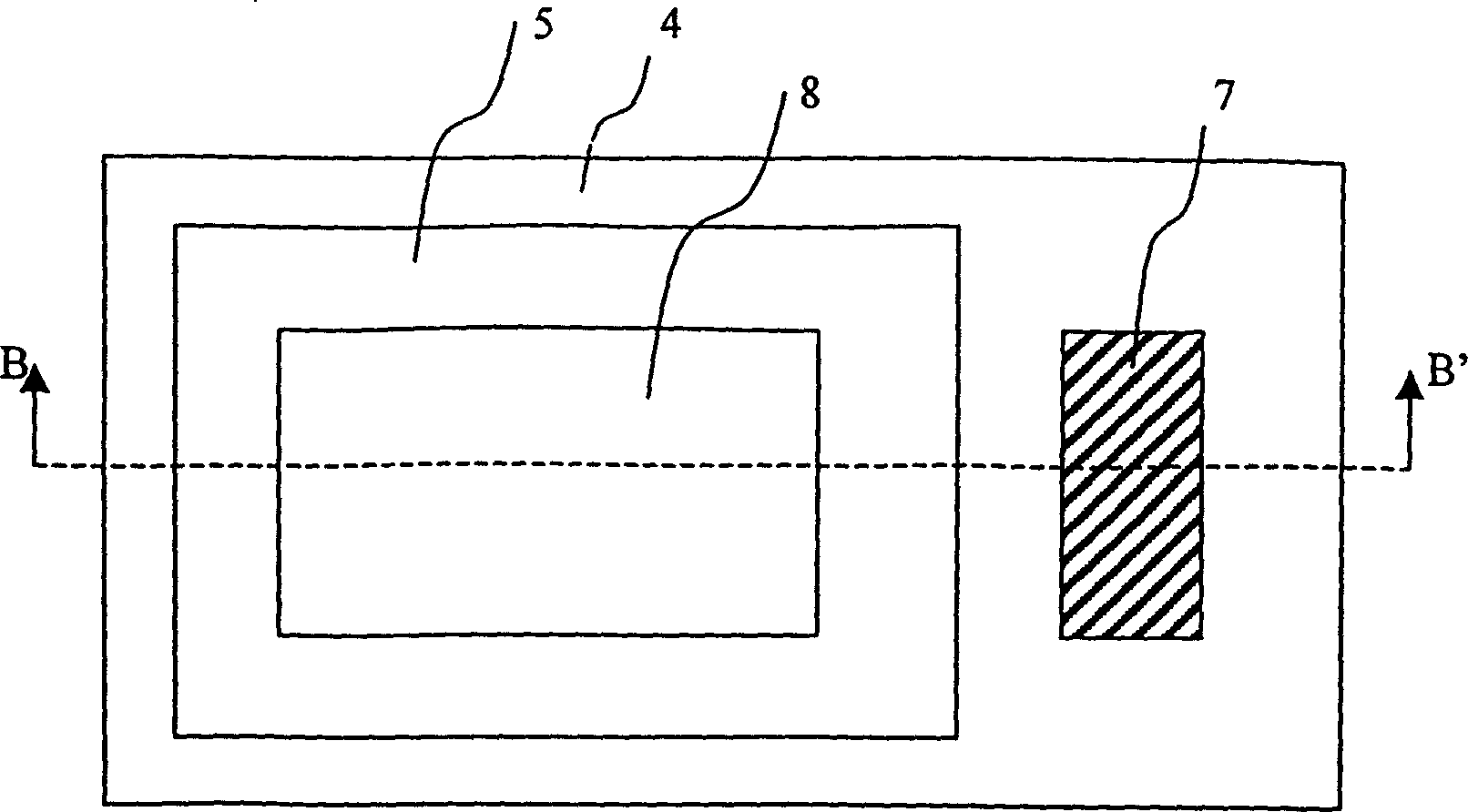
[0032] figure 2 A plan view showing a first embodiment of the electrode configuration of the present invention for the lowermost LED of the stack package. image 3 along figure 2 Sectional view of line BB'. The substrate 1 is generally an opaque group III-V or II-VI compound semiconductor such as GaAS, GaP or GaN. On substrate 1, one layer of n-type semiconductor layer 2 is epitaxy by epitaxy technology (see ...


PUM

PropertyMeasurementUnit
Widthaaaaaaaaaa
Widthaaaaaaaaaa
Widthaaaaaaaaaa

Abstract

This invention discloses a structure of LED electrode and its manufacturing method. After forming a pn contact surface LED on the baseplate, a layer of silicon oxide is formed around the grain and onthe cut-path part, and deposited by a transparent conductive layer and a layer of Au or AuGe on it, or and opening an open-end at the center; after contacting with heated and alloy formed ohm, a longstrip of Al, Al alloy or Au connecting wire pad is formed at a side of the grain for writing and used as the LED positive electrode, and the negative electrode is formed on the substrate by metal contact. The other structure is that both positive and negative electrodes are on the front with etched pn interface p-type layer, and negative electrode is formed with n-type material and positive electrode with p-type material.

Description

technical field [0001] The present invention relates to the electrode structure and manufacturing method of semiconductor light-emitting diode (LED), in particular to the electrode structure and manufacturing method of LED suitable for stack packaging. Background technique [0002] A light emitting diode (Light Emitted Diode, LED) is a semiconductor component that emits light, and is formed with a pn junction to convert electrical energy into light. It has the characteristics of small size, long life, low driving voltage, fast response, shock resistance, heat resistance, etc., and can meet the needs of light, thin, and miniaturized various application equipment, and is used for various traffic signs, event billboards, and LCD backlights. Light source and other products widely used in daily life. [0003] Light-emitting diodes use various compound semiconductor materials such as III-V materials, II-VI materials, etc., and are designed with different structures such as pn jun...

Claims


Application Information

Patent Timeline
IPC IPC(8): H01L33/36H01L33/38
Inventor 张修恒
Owner 张修恒
Why Eureka
Try Eureka