Plasma processing device and method thereof

A plasma and processing device technology, which is applied in the field of plasma processing devices, can solve problems such as cracks in the dielectric film, peeling of the dielectric film, substrate turnover, etc., and achieve the effect of suppressing abnormal discharge

Inactive Publication Date: 2004-02-25
TOKYO ELECTRON LTD
View PDF0 Cites 5 Cited by
  • Summary
  • Abstract
  • Description
  • Claims
  • Application Information

AI Technical Summary

Problems solved by technology

[0004] However, the dielectric film formed on the electrode is necessary for plasma corrosion resistance, and is often used as a high-priced ceramic material with high corrosion resistance, and must be able to withstand the DC voltage and plasma applied to the electrode due to its thickness. Insulation between, so the cost of the electrostatic chuck becomes extremely high
In addition, if the LCD glass substrate is enlarged, the dielectric film will be peeled off due to the difference in thermal expansion coefficient between the metal material constituting the main body of the substrate holding table and the ceramic material constituting the dielectric film, and cracks will appear on the dielectric film. Problems such as cracks, substrate holding table itself flipping, etc.
[0005] In order to avoid such problems, the LCD glass substrate itself is a dielectric body, and it is considered to hold the LCD glass substrate on the electrodes without using a dielectric film. A slight gap is formed between the substrate and the electrode on the peripheral portion, and since the electrode is exposed on the gap, a DC discharge is generated by applying a DC voltage for adsorption.

Method used


Image

  • Plasma processing device and method thereof
  • Plasma processing device and method thereof
  • Plasma processing device and method thereof

Examples


Embodiment Construction

[0024] Embodiments of the present invention will be described below with reference to the drawings.

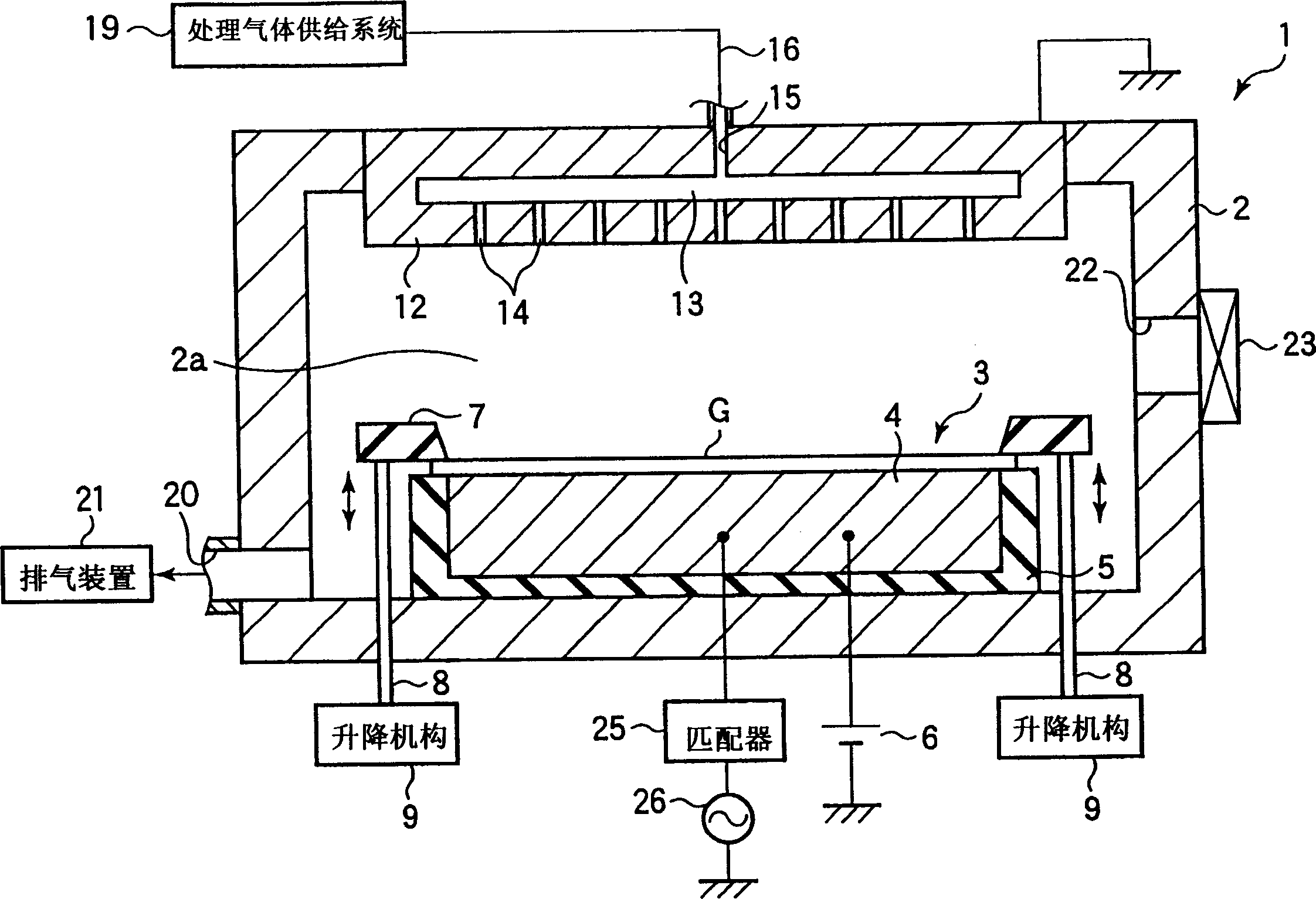
[0025] figure 1 It is a plasma etching apparatus for LCD glass substrates which schematically shows the embodiment of this invention. The plasma etching apparatus 1 is configured as a capacitively coupled parallel plate plasma etching apparatus.

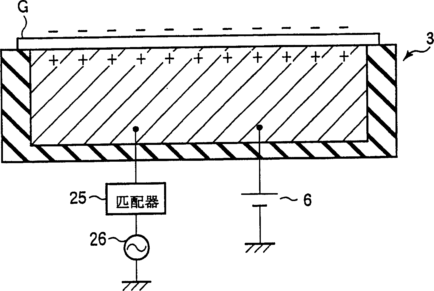
[0026] The plasma etching device 1 has a rectangular box-shaped chamber 2 whose surface is made of anodized aluminum. A substrate holding table 3 for holding an LCD glass substrate G as a dielectric substrate to be processed is provided on the bottom of the chamber 2 . The substrate holding table 3 has a holding table main body 4 formed of a conductor such as aluminum, and an insulating member 5 covering the side surfaces and the bottom surface of the holding table main body 4 . When the substrate G is placed, the upper surface of the holding table main body 4 becomes the substrate mounting surface, and the periphery of the substr...


PUM

PropertyMeasurementUnit
lengthaaaaaaaaaa
thicknessaaaaaaaaaa

Abstract

The plasma treatment device, which performs plasma treatment on a dielectric substrate G to be treated, is provided with the electrode 4 on which the substrate G is placed directly, a pressing mechanism 7 which presses the peripheral edge of the substrate G placed on the electrode 4 toward the electrode 4, and a treatment gas supplying mechanism 19 which supplies a process gas to the periphery of the substrate G. The treatment device is also provided with a plasma-generating means 26, which generates a plasma of the process gas in the periphery of the substrate G and and a DC power source 6, which is connected to the electrode 4 and impresses the DC voltage upon the electrode 4. While the pressing mechanism 7 presses the peripheral edge of the substrate G placed on the electrode 4, the substrate G is sucked to the electrode 4 by impressing the DC voltage on the electrode 4.

Description

technical field [0001] The present invention relates to a plasma processing apparatus and a plasma processing method for performing plasma processing such as etching on a substrate to be processed. Background technique [0002] In the manufacturing process of a liquid crystal display device, a plasma processing apparatus such as a plasma etching apparatus or a plasma CVD film formation apparatus is used to perform etching or film formation on a glass substrate as a substrate to be processed. [0003] In such a plasma processing apparatus, plasma is generated by appropriate means while the LCD glass substrate is held on a substrate holding table, and plasma processing is performed. As such a holding mechanism, a crank mechanism that mechanically presses the periphery of the LCD glass substrate is currently used. However, if a heat transfer gas is introduced between the substrate and the substrate holding table to control the temperature of the substrate, the center of the sub...

Claims


Application Information

Patent Timeline
Patent Type & Authority Applications(China)
IPC IPC(8): H05H1/46C23C16/458G02F1/13H01L21/00H01L21/205H01L21/3065
CPCH01J37/3244
Inventor 里吉务
Owner TOKYO ELECTRON LTD
Why Eureka
Try Eureka