High purity copper sputtering target material
A sputtering target, high-purity technology, used in sputtering plating, metal material coating process, electrical components, etc. Line film and other problems, to achieve the effect of suppressing abnormal discharge and stabilizing film formation
- Summary
- Abstract
- Description
- Claims
- Application Information
AI Technical Summary
Problems solved by technology
Method used
Image
Examples
no. 3 Embodiment approach
[0131] Hereinafter, the high-purity copper sputtering target material which concerns on 3rd Embodiment of this invention is demonstrated.
[0132] Since the usage as the high-purity copper sputtering target material of this embodiment is the same as that of 1st Embodiment, it omits.
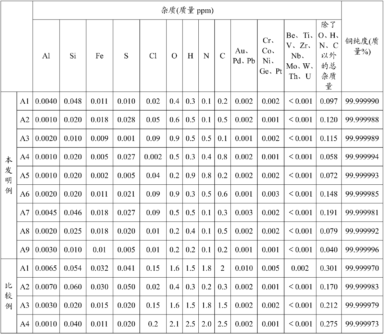
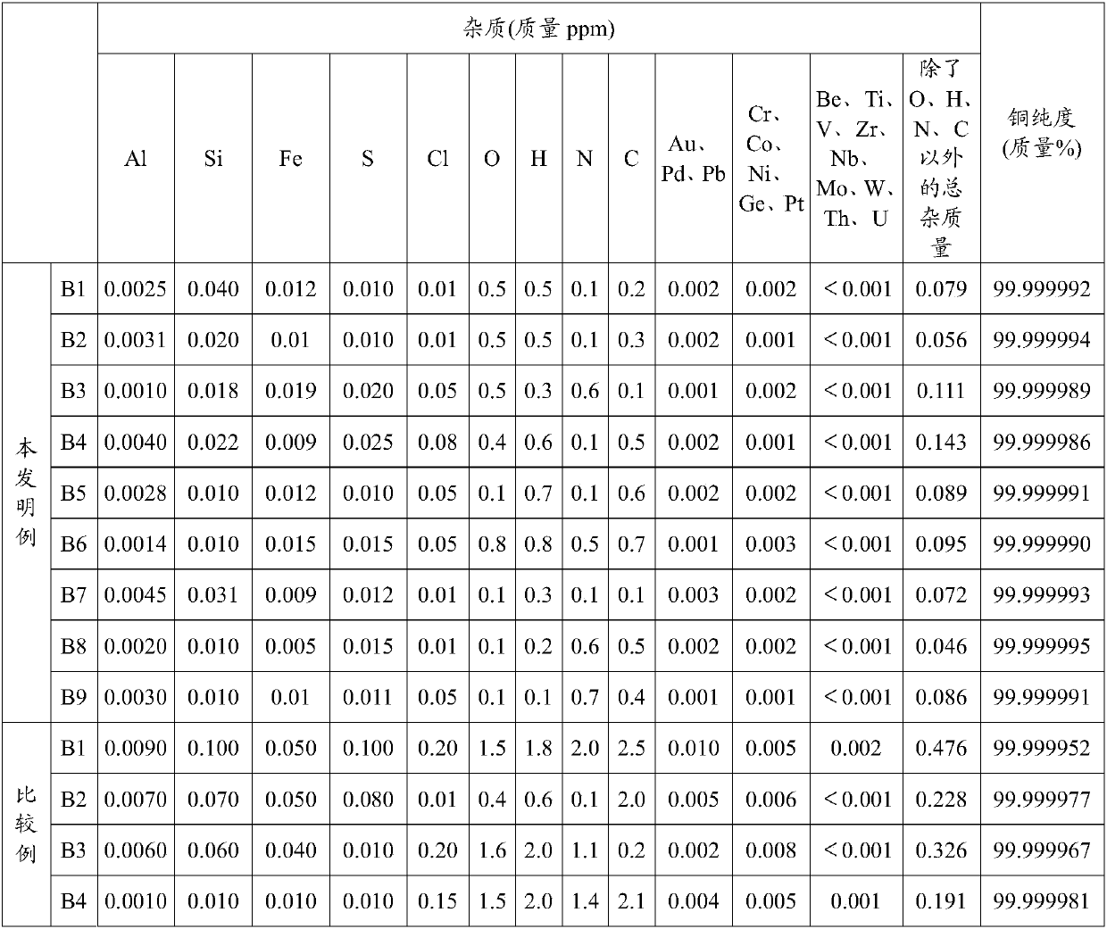
[0133] Since the composition of the high-purity copper sputtering target material which is this embodiment is the same as the composition of the high-purity copper sputtering target material of 1st Embodiment, the detailed description is abbreviate|omitted.
[0134] And, in the high-purity copper sputtering target material as the present embodiment, by thermal desorption gas analyzer (TDS-MS) at 1 × 10 -7 The sample extracted from the target to a predetermined size is heated in an ultra-high vacuum below Pa, and the gas components released during the period from 50°C to 1000°C are ionized by the electron impact method, and analyzed by a quadrupole mass spectrometer. The generated ions are analyz...
no. 4 Embodiment approach
[0163] Hereinafter, the high-purity copper sputtering target material which concerns on 4th Embodiment of this invention is demonstrated.
[0164] Since the usage as the high-purity copper sputtering target material of this embodiment is the same as that of 1st Embodiment, it omits.
[0165] Since the composition of the high-purity copper sputtering target material which is this embodiment is the same as the composition of the high-purity copper sputtering target material of 1st Embodiment, the detailed description is abbreviate|omitted.
[0166] In addition, in the high-purity copper sputtering target according to the present embodiment, the average value of local orientation differences in crystal orientation between one measurement point and all other measurement points in the same crystal grain obtained by EBSD measurement The value (GOS) is set to 4° or less.
[0167] And in the high-purity copper sputtering target material which is this embodiment, an average crystal gr...
no. 5 Embodiment approach
[0195] Hereinafter, the high-purity copper sputtering target material which concerns on 5th Embodiment of this invention is demonstrated.
[0196] Since the usage as the high-purity copper sputtering target material of this embodiment is the same as that of 1st Embodiment, it omits.
[0197] Since the composition of the high-purity copper sputtering target material which is this embodiment is the same as the composition of the high-purity copper sputtering target material of 1st Embodiment, the detailed description is abbreviate|omitted.
[0198] In addition, in the high-purity copper sputtering target according to the present embodiment, the area ratio of crystals having a plane orientation of ±10° on the sputtering surface of the target obtained by EBSD measurement is set to 0.2 or less.
[0199] And in the high-purity copper sputtering target material which is this embodiment, an average crystal grain diameter is made into 70 micrometers or less, and Vickers hardness is ma...
PUM
 Abstract
Description
Claims
Application Information


