

Sintered oxide material, target comprising same, and oxide semiconductor thin film
A technology of oxide semiconductors and oxides, which is applied in semiconductor devices, semiconductor/solid-state device manufacturing, transistors, etc., can solve problems such as insufficient target research, and achieve the effects of suppressing abnormal discharge and stable reproducibility
- Summary
- Abstract
- Description
- Claims
- Application Information
AI Technical Summary
Problems solved by technology
Method used
Image

Examples
Embodiment 1-3
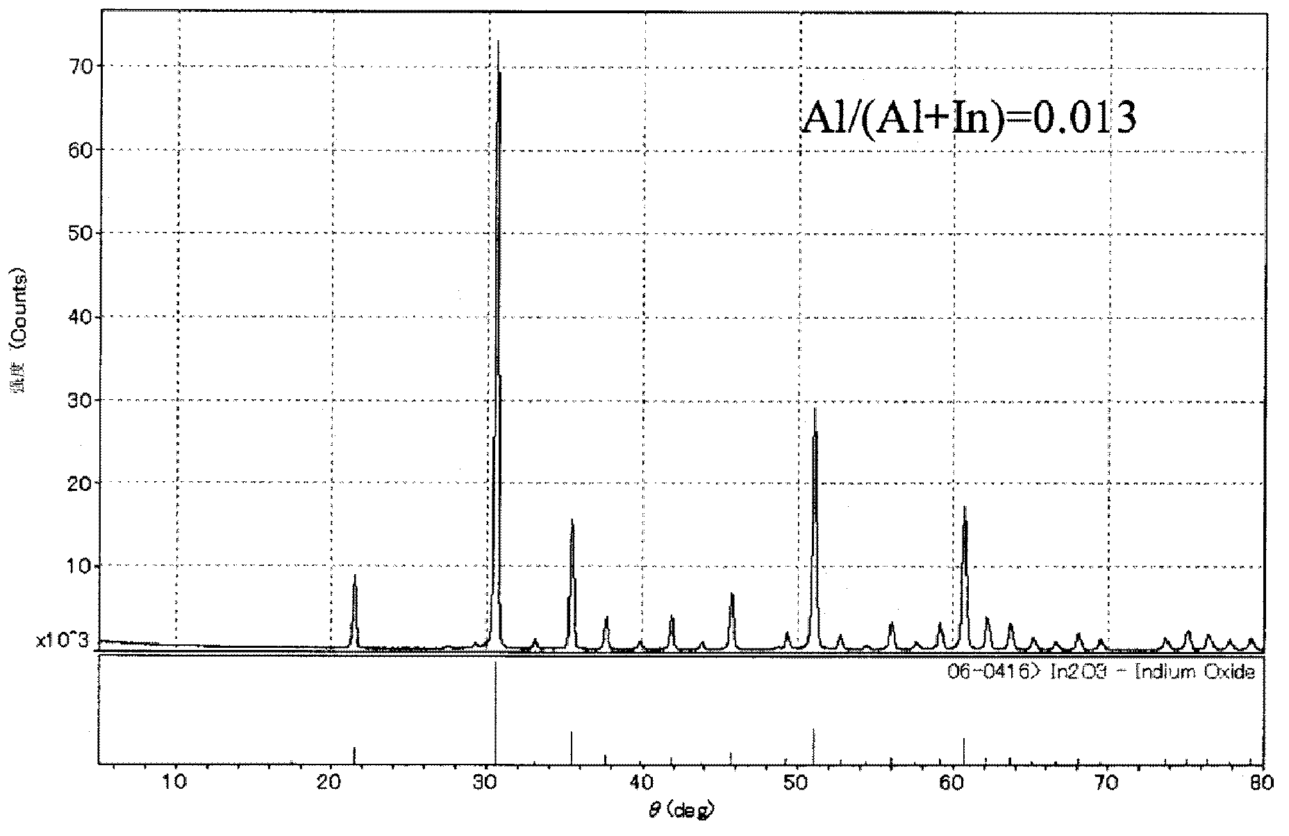
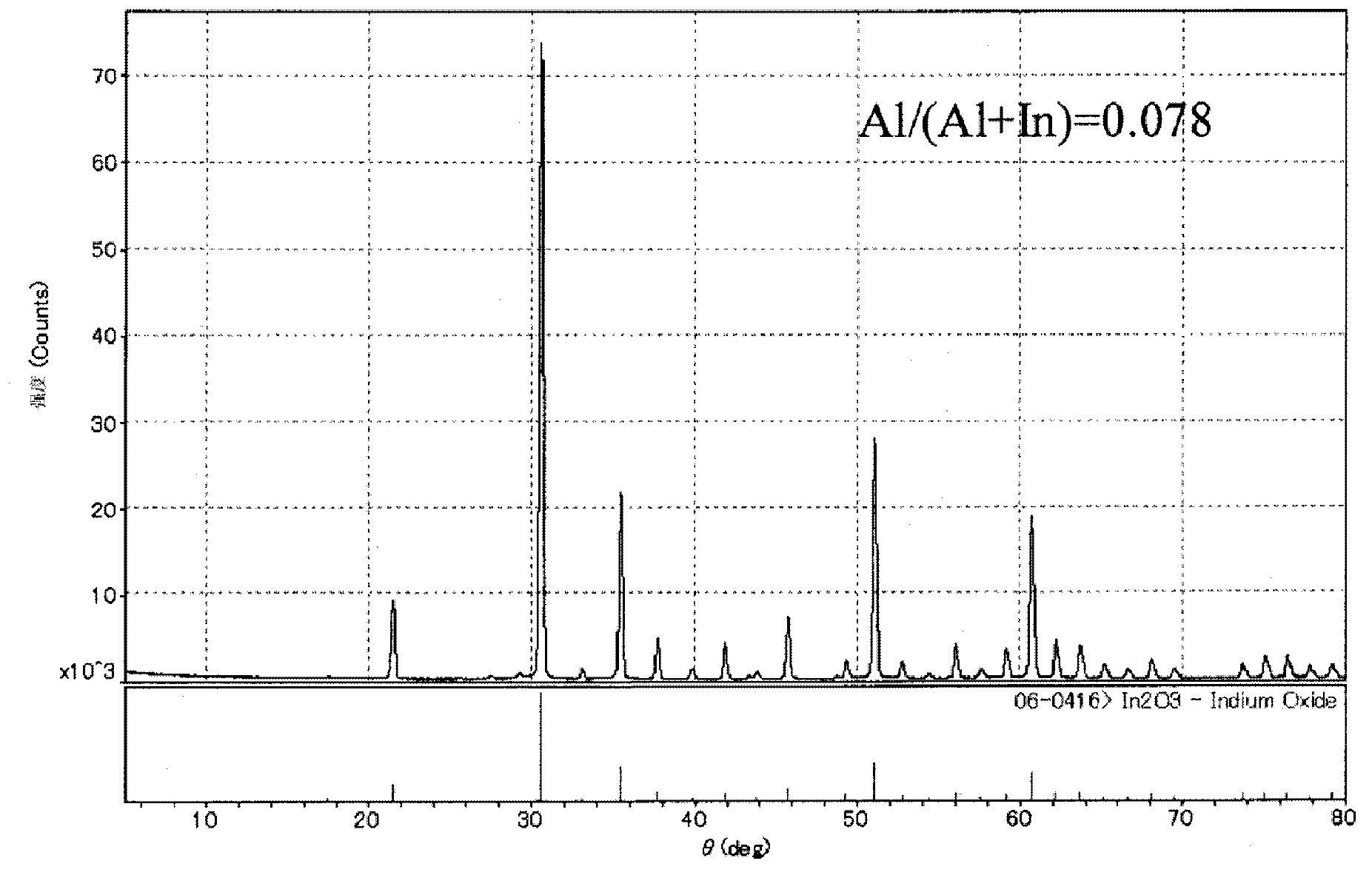
[0121] Weigh the indium oxide powder with an average particle diameter of 0.98 μm and the alumina powder with an average particle diameter of 0.97 μm to obtain the atomic ratio Al / (Al+In) shown in Table 1. After uniformly pulverizing and mixing, add the bonding agent for molding. The agent is granulated. Next, the raw material mixed powder was uniformly filled into a mold, and compression molding was performed at a pressure of 140 MPa with a cold press. The molded body thus obtained was fired in a sintering furnace at the firing temperature and firing time shown in Table 1 to produce a sintered body.
[0122] The firing atmosphere was an oxygen atmosphere during the temperature rise, and was also in the air (atmosphere), and the firing was performed at a temperature rise rate of 1° C. / min and a temperature fall rate of 15° C. / min.
[0123] In addition, the average particle diameter of the raw material oxide powder used was measured with the laser diffraction particle size dis...
Embodiment 4
[0158] On a glass substrate and with a 100nm thick thermal oxide film (SiO 2 ) were respectively used on the silicon substrates obtained in Example 1 (Al / (In+Al)=0.013), and a thin film with a film thickness of 50 nm was formed by DC magnetron sputtering.
[0159] Sputtering is vacuum exhausted until the back pressure reaches 1×10 -4 Pa, while argon 9.9sccm, water 0.1sccm (hydraulic pressure: 4.0×10 -3 Pa) was flowed in, and the pressure was adjusted to 0.4 Pa, and the sputtering power was 100W at room temperature.
[0160] The crystal structure immediately after film formation of the thin film formed on the glass substrate was confirmed by XRD. As a result, no clear diffraction peak was observed, and it was confirmed that it was amorphous. The glass substrate on which the thin film was formed was put into a heating furnace heated to 300° C. in air, and treated for 1 hour. As a result of XRD measurement of the annealed thin film, only the peak of the bixbyite structure of ...
Embodiment 5
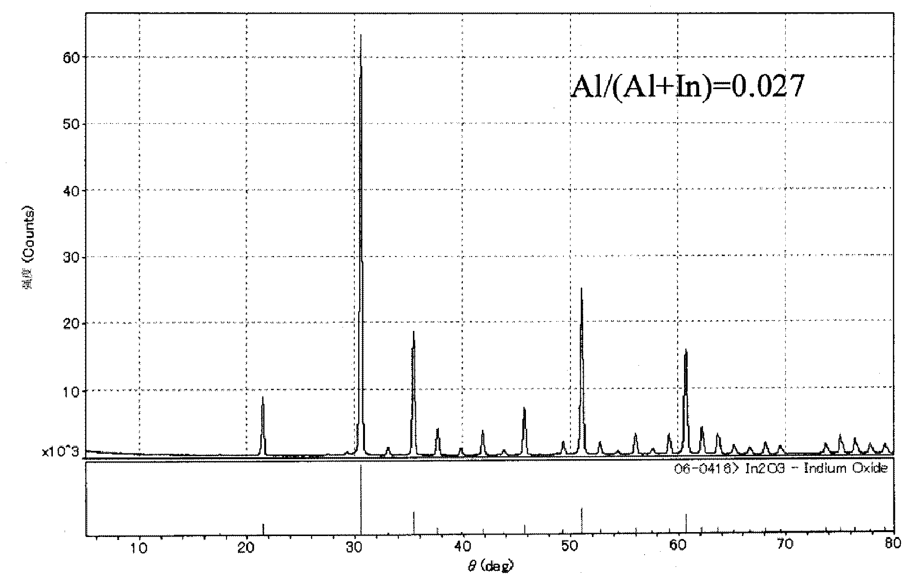
[0165] On a glass substrate and with a 100nm thick thermal oxide film (SiO 2 ) on silicon substrates, respectively using the target (Al / (In+Al)=0.027) obtained in Example 2, a thin film with a film thickness of 50 nm was formed by DC magnetron sputtering.
[0166] Sputtering is vacuum exhausted until the back pressure reaches 1×10 -4 Pa, while argon 9.9sccm, water 0.1sccm (hydraulic pressure: 4.0×10 -3 Pa) was flowed in, and the pressure was adjusted to 0.4 Pa, and the sputtering power was 100W at room temperature.
[0167] The crystal structure immediately after film formation of the thin film formed on the glass substrate was confirmed by XRD. As a result, no clear diffraction peak was observed, and it was confirmed that it was amorphous. The glass substrate on which the thin film was formed was put into a heating furnace heated to 300° C. in air, and treated for 1 hour. As a result of XRD measurement of the annealed thin film, only the peak of the bixbyite structure of ...
PUM
| Property | Measurement | Unit |
|---|---|---|
| particle diameter | aaaaa | aaaaa |
| density | aaaaa | aaaaa |
| density | aaaaa | aaaaa |
Abstract
Description
Claims
Application Information