Copper material for high-purity copper sputtering target, and high-purity copper sputtering target

A sputtering target and high-purity technology, applied in the field of copper raw materials for high-purity copper sputtering targets and high-purity copper sputtering targets, can solve the problem of rising manufacturing costs and the inability to stably form miniaturized and thinned wiring films , abnormal discharge and other problems, to achieve the effect of low cost, suppression of abnormal discharge, and stable film formation

Active Publication Date: 2016-02-17
MITSUBISHI MATERIALS CORP
View PDF8 Cites 3 Cited by
  • Summary
  • Abstract
  • Description
  • Claims
  • Application Information

AI Technical Summary

Problems solved by technology

However, the reduction of foreign matter by these alone is still insufficient, and abnormal discharge (arc discharge) may occur during film formation, making it impossible to stably form a miniaturized and thinned wiring film.
[0010] In addition, in order to reduce the impurities in the sputtering target, it is also considered to use 8N copper with a purity of 99.999999% by mass or more, but when producing a copper raw material with such a purity, it is necessary to repeat the purification treatment process three times or more, so Leading to a substantial increase in manufacturing costs and other issues

Method used


Image

  • Copper material for high-purity copper sputtering target, and high-purity copper sputtering target
  • Copper material for high-purity copper sputtering target, and high-purity copper sputtering target

Examples


Embodiment

[0077] Hereinafter, the result of the evaluation test which evaluated the copper raw material for high-purity copper sputtering targets of embodiment mentioned above, and a high-purity copper sputtering target is demonstrated.

[0078] (Example 1-5 of the present invention)

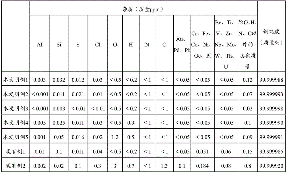
[0079] Using electrolytic copper whose Al content is 1 mass ppm or less, Si content is 1 mass ppm or less, and other impurities (other than O, H, N, and C) are 20 mass ppm or less as a raw material, under the electrolytic purification conditions exemplified in the embodiment Electrolytic purification was repeated twice to produce a copper raw material (copper raw material).

[0080] The raw material produced by the above-mentioned production method was charged into a crucible made of high-purity carbon (carbon crucible), and vacuum melting was carried out at 1130° C. (pressure 10 -5 Pa). In addition, after melting under vacuum, it was held at a temperature of 1150° C. for 30 minutes. Thereafter, in a v...

example 1

[0083] Using electrolytic copper with Al content of 2 mass ppm or less, Si content of 3 mass ppm or less, and other impurities (other than O, H, N, and C) of 20 mass ppm or less as the raw material, repeated electrolysis using copper nitrate electrolyte Purification was performed twice to obtain a copper raw material having an Al content of 0.005 mass ppm and a Si content of 0.06 mass ppm.

[0084] The raw material produced by the above-mentioned production method was put into a carbon crucible, melted at 1130°C in an Ar atmosphere, and held at a temperature of 1150°C for 30 minutes. Thereafter, the melted raw material was poured into a carbon mold in an Ar atmosphere to produce a high-purity copper ingot with a diameter of 200 mm×a height of 800 mm. Table 1 shows the composition of the obtained ingot.

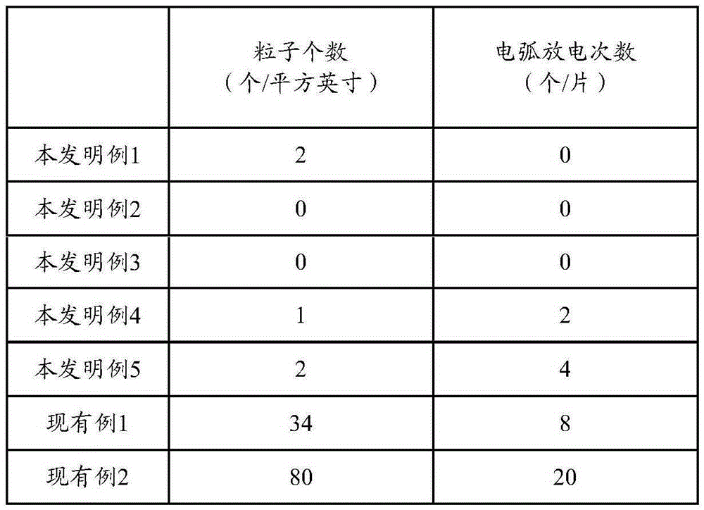
[0085] The manufactured high-purity copper ingot is forged at 500°C, the obtained high-purity forged block is cut into a diameter of 300mm×height of 15mm, and the cut out for...


PUM

PropertyMeasurementUnit
particle diameteraaaaaaaaaa

Abstract

This copper material for a high-purity copper sputtering target is such that the purity of Cu excluding O, H, N, and C is in a range of 99.999980 to 99.999998 mass%, the Al content is 0.005 mass ppm or less, and the Si content is 0.05 mass ppm or less.

Description

technical field [0001] The present invention relates to a high-purity copper sputtering target copper raw material and high Pure copper sputtering target. [0002] This application claims the priority based on the patent application 2013-145733 for which it applied to Japan on July 11, 2013, and the patent application 2014-116011 for which it applied in Japan on June 4, 2014, and uses the content here. Background technique [0003] Conventionally, Al has been widely used as wiring films in semiconductor devices, flat panel displays such as liquid crystal and organic EL panels, and touch panels. Recently, the miniaturization (narrow width) and thinning of wiring films have been achieved, and wiring films with lower specific resistance than conventional ones are required. [0004] Then, along with the miniaturization and thinning of the above-mentioned wiring film, there is provided a wiring film made of copper (Cu), which is a material having a specific resistance lower tha...

Claims


Application Information

Patent Timeline
Patent Type & Authority Applications(China)
IPC IPC(8): C25C1/12C23C14/34H01L21/28H01L21/285C22C9/00
CPCC25C1/12C22C9/00C23C14/3414C22C1/02H01J37/3426H01J2237/081H01J2237/3323
Inventor 樱井晶谷雨佐藤雄次熊谷训
Owner MITSUBISHI MATERIALS CORP
Why Eureka
Try Eureka