

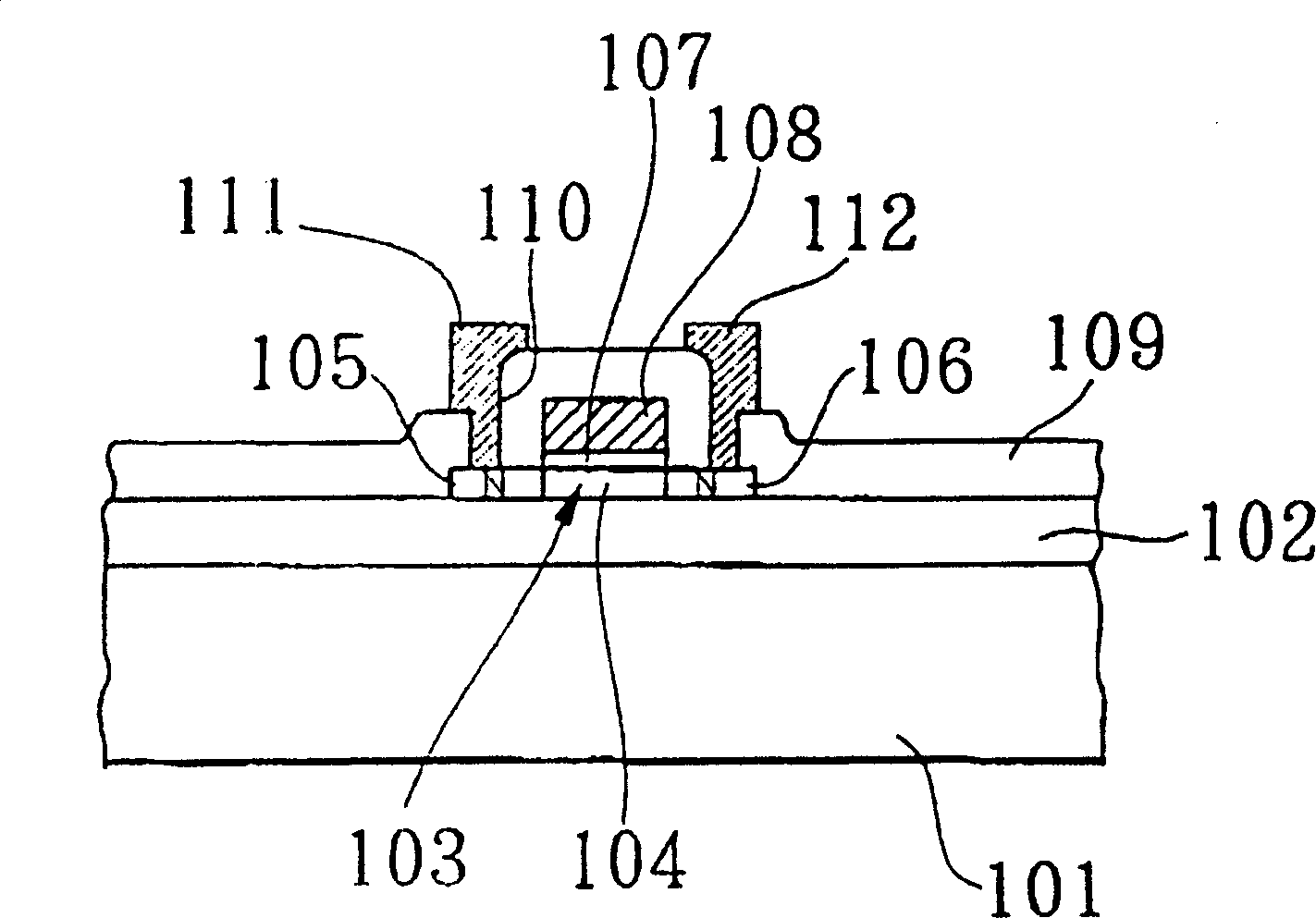
Method for producing thin film transistor
A technology of thin film transistors and manufacturing methods, applied in the direction of transistors, semiconductor/solid-state device manufacturing, semiconductor devices, etc., can solve problems such as inability to improve crystal defects, achieve the effect of improving crystal defects and preventing discrete
- Summary
- Abstract
- Description
- Claims
- Application Information
AI Technical Summary
Problems solved by technology
Method used
Image

Examples
no. 1 example
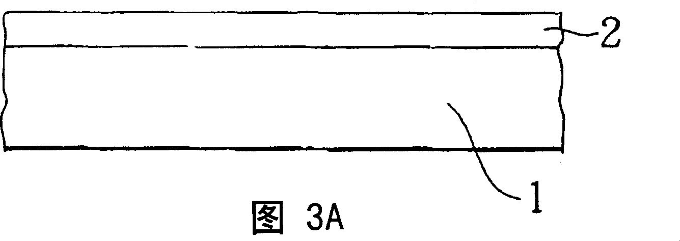
[0034] Figure 3A to Figure 3K is a sectional view of the thin film transistor in each step of the thin film transistor manufacturing method according to the first embodiment. Figure 4 is a temperature profile when performing thermal annealing in this method, and the method of manufacturing a thin film transistor will be explained below based on the first embodiment.
[0035] An N-channel type thin film transistor having a top gate structure is fabricated in the first embodiment.
[0036] First, as shown in FIG. 3A, a base film 2 is formed on an electrically insulating substrate by chemical vapor deposition (CVD). The substrate is composed of a glass substrate with a thickness of about 0.7 mm. The base film 2 is composed of a silicon oxide film with a thickness of about 300 nm. The base film 2 serves as a buffer film to prevent impurities that adversely affect the characteristics of the thin film transistor from entering the thin film semiconductor layer described later fr...
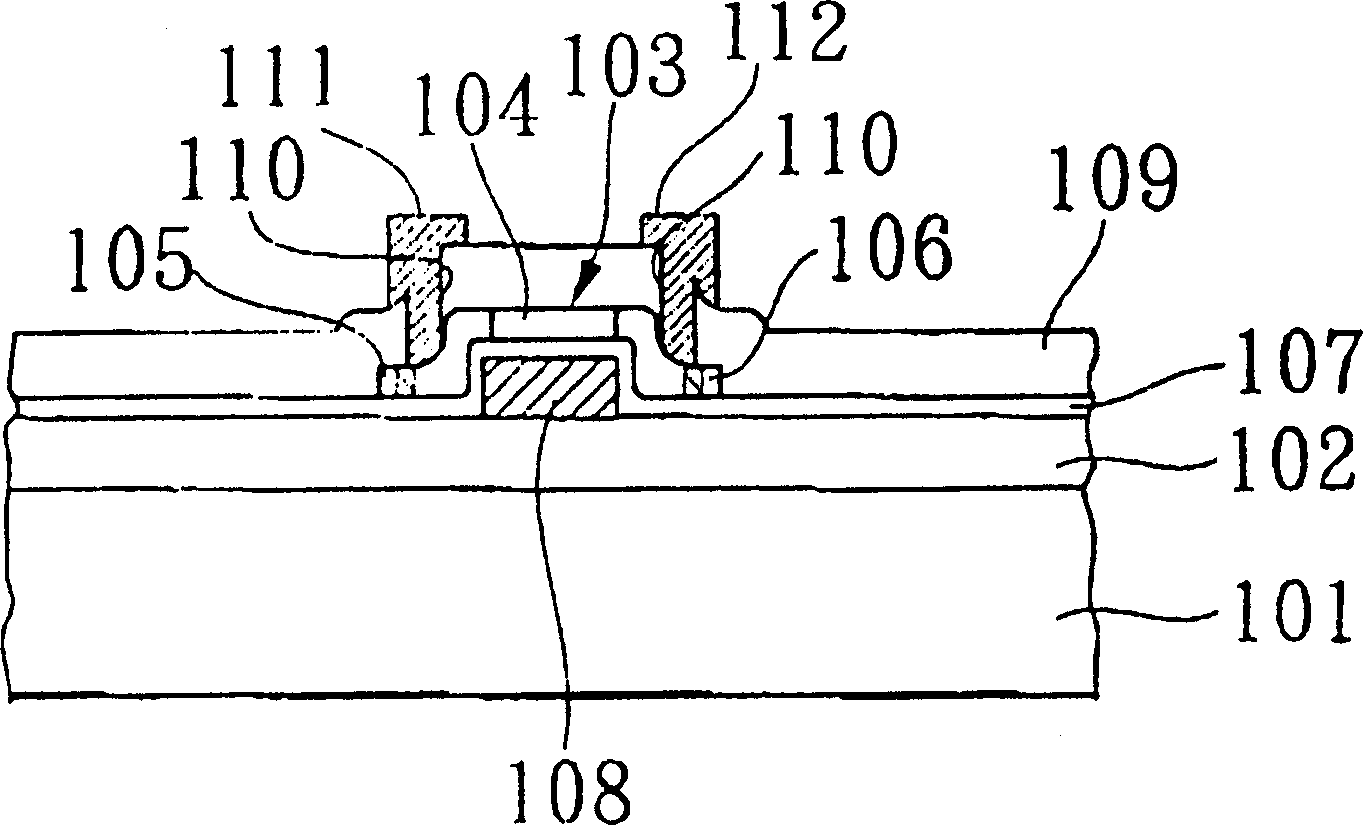
no. 2 example
[0059] Figure 5A and 5B is a sectional view of the thin film transistor in the main steps of the manufacturing method of the thin film transistor according to the second embodiment.
[0060] Those parts and elements corresponding to those of the first embodiment are designated with the same reference numerals and operate in the same manner as the corresponding parts and elements of the first embodiment, unless otherwise specified.
[0061] The second embodiment differs from the first embodiment in that the interlayer insulating film is designed to have a multilayer structure.
[0062] Specifically, as Figure 5A shown in reference to Figure 3K After the explained steps, second interlayer insulating film 17 is formed on the entire surface of substrate 1 by CVD. The second interlayer insulating film 17 is made of silicon nitride and has a thickness of about 400 nm. The second interlayer insulating film 17 and the interlayer insulating film 13 define a multilayer interlaye...
no. 3 example
[0070] Figure 6A to Figure 6Iis a cross-sectional view of the thin film transistor in each step of the thin film transistor manufacturing method according to the third embodiment. Refer to the following Figure 6A to Figure 6I A method of manufacturing the thin film transistor according to the third embodiment is explained.
[0071] The third embodiment differs from the first embodiment in that the third embodiment is applied to a thin film transistor having a bottom gate structure whereas the first embodiment is applied to a thin film transistor having a top gate structure.
[0072] First, if Figure 6A As shown, base film 22 is formed on insulating substrate 21 by CVD. The substrate 21 is composed of a glass substrate having a thickness of about 0.7 mm. Base film 22 is composed of a silicon oxide film having a thickness of about 400 nm. The base film 22 is used as a buffer film to prevent impurities that adversely affect the thin film transistor from invading from the ...
PUM
| Property | Measurement | Unit |
|---|---|---|
| thickness | aaaaa | aaaaa |
| thickness | aaaaa | aaaaa |
| thickness | aaaaa | aaaaa |
Abstract
Description
Claims
Application Information