
Integrated circuit with nonvoltile data memory circuit

A technology of integrated circuits and latch circuits, applied to logic circuits, digital memory information, circuits, etc. using basic logic circuit components, can solve problems such as easy data inversion, reduce the area of ​​circuit elements, reduce the The effect of simplifying the design

Inactive Publication Date: 2004-04-14
FUJITSU SEMICON LTD
View PDF1 Cites 16 Cited by
  • Summary
  • Abstract
  • Description
  • Claims
  • Application Information

AI Technical Summary

Problems solved by technology

[0015] However, in the nonvolatile latch circuit used in the nonvolatile SRAM of Non-Patent Document 2, when the power is turned on again, there arises a problem in that due to the irregularity of the transistor characteristics of the latch circuit, recovery data is prone to inversion
However, the latch circuit in this application does not use MTCMOS technology

Method used


Image

  • Integrated circuit with nonvoltile data memory circuit
  • Integrated circuit with nonvoltile data memory circuit
  • Integrated circuit with nonvoltile data memory circuit

Examples


Embodiment Construction

[0043] An embodiment of the present invention will be described below with reference to the drawings. However, the protection scope of the present invention is not limited to the following embodiments, but encompasses the scope defined by the appended claims and their equivalents.

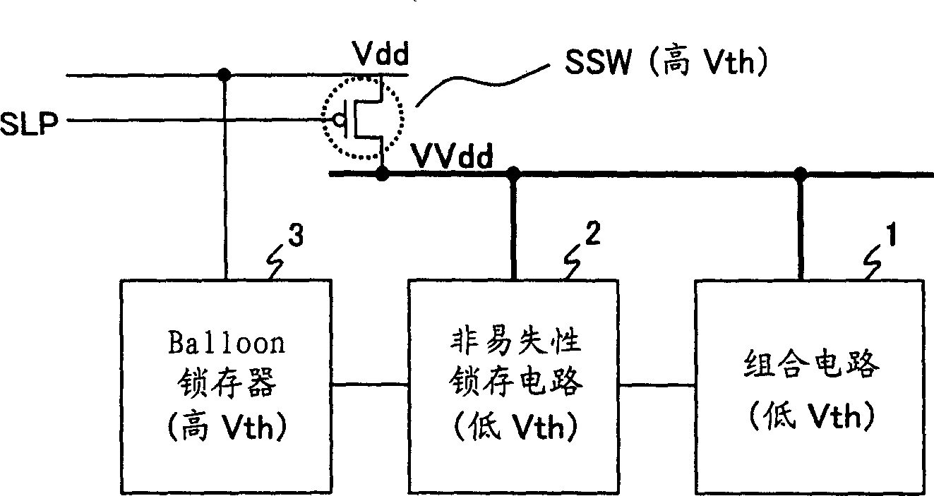
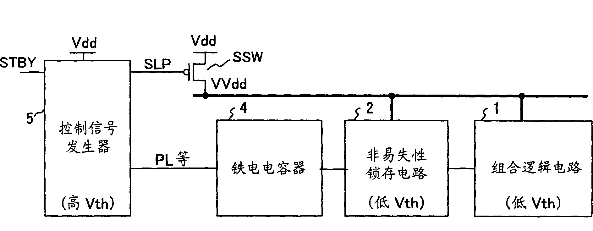
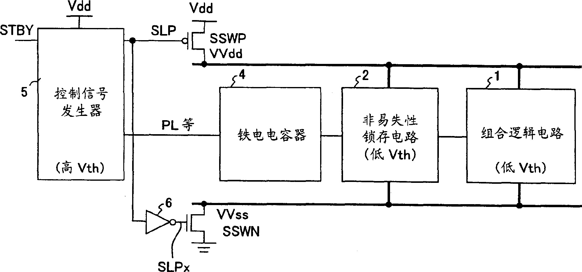
[0044] figure 2 It is the schematic diagram of the structure of the integrated circuit in this embodiment. Similar to the example in Fig. 1, the normal power supply Vdd and the virtual power supply VVdd are connected through a sleep switch SSW, and the combinational logic circuit 1 and the non-volatile latch circuit 2 are connected to the virtual power supply VVdd. The sleep switch SSW is composed of high Vth transistors, whereas the combinational logic circuit 1 and the nonvolatile latch circuit 2 are composed of low Vth transistors.

[0045] The ferroelectric capacitor 4 is provided in the integrated circuit of this embodiment to hold the data held in the nonvolatile latch circuit 2 even when t...


PUM


Abstract

An integrated circuit has a sleep switch, provided between a first power line and a second power line, which is constituted by a transistor of a first threshold voltage, and which becomes non-conducting in a sleep mode, and further has a latch circuit, connected to the second power line, which is constituted by a transistor of a second threshold voltage which is lower than the first threshold voltage, and a ferroelectric capacitor for storing data held in the latch circuit in accordance with the polarization direction of a ferroelectric film thereof. The integrated circuit also comprises a control signal generating circuit which, when returning to an active mode from the sleep mode, generates a plate signal for driving a terminal of the ferroelectric capacitor to generate a voltage in the latch circuit in accordance with the polarization direction, and generates a sleep signal for causing the sleep switch to conduct to thereby activate the latch circuit following the driving of the ferroelectric capacitor.

Description

[0001] This application is based on and claims the benefit of priority from Japanese Patent Application No. 2002-247346 filed on August 27, 2002, the entire contents of which are incorporated herein by reference. technical field [0002] The present invention relates to an integrated circuit having a non-volatile data storage circuit in multi-threshold voltage CMOS to achieve low power consumption, and in particular, the present invention relates to an integrated circuit capable of simplifying power supply layout and avoiding errors in data recovery operations operating integrated circuits. Background technique [0003] Multi-threshold voltage CMOS (MTCMOS) has been proposed as a technology for reducing power consumption in LSI (Large Scale Integration). According to this MTCMOS technology, for example, as described in Non-Patent Document 1 below, high-current drive capability of low-Vth transistors and low leakage quality of high-Vth transistors are used to realize high-spe...

Claims


Application Information

Patent Timeline
Patent Type & Authority Applications(China)
IPC IPC(8): H01L21/822G11C14/00G11C16/34H01L21/82H01L27/04H03K19/00H03K19/173H03K19/185
CPCG11C14/00G11C14/0072G11C16/34
Inventor 横关亘桝井昇一
Owner FUJITSU SEMICON LTD
Learn More