

Silicon seed crystal for straight drawing monocrystal growth and its process
A processing method, silicon single crystal technology, applied in the direction of single crystal growth, crystal growth, chemical instruments and methods, etc., can solve the problems of increased manufacturing cost, unsafety, easy fracture of seed crystal, etc., so as to reduce processing cost and prolong The effect of service life
- Summary
- Abstract
- Description
- Claims
- Application Information
AI Technical Summary
Problems solved by technology
Method used
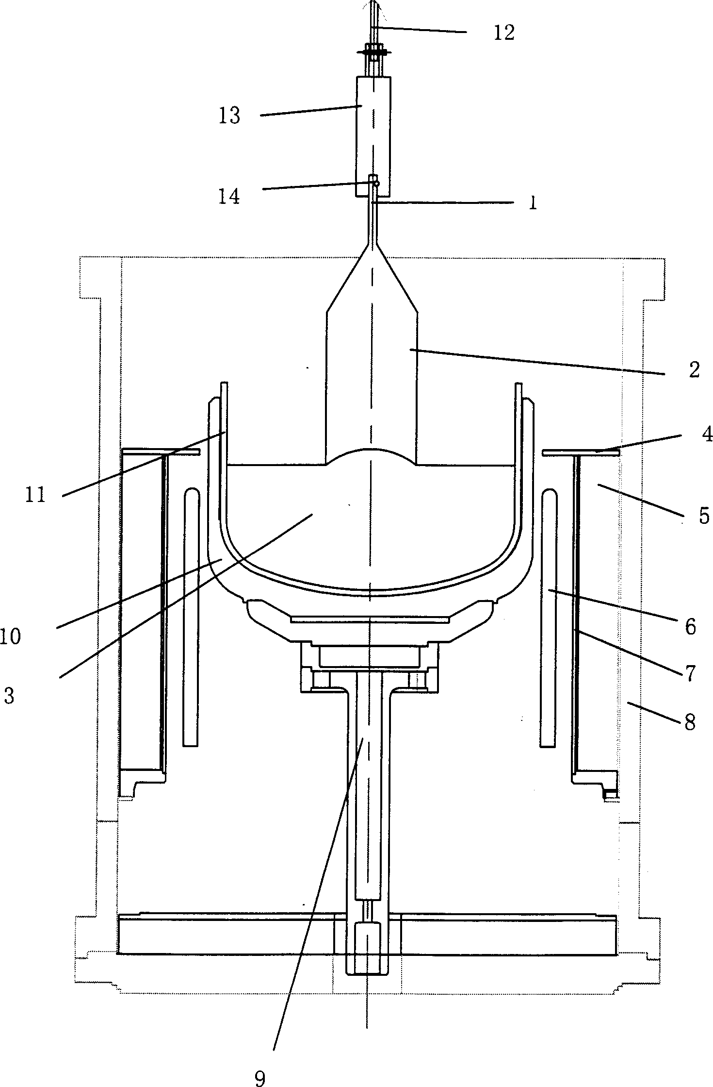
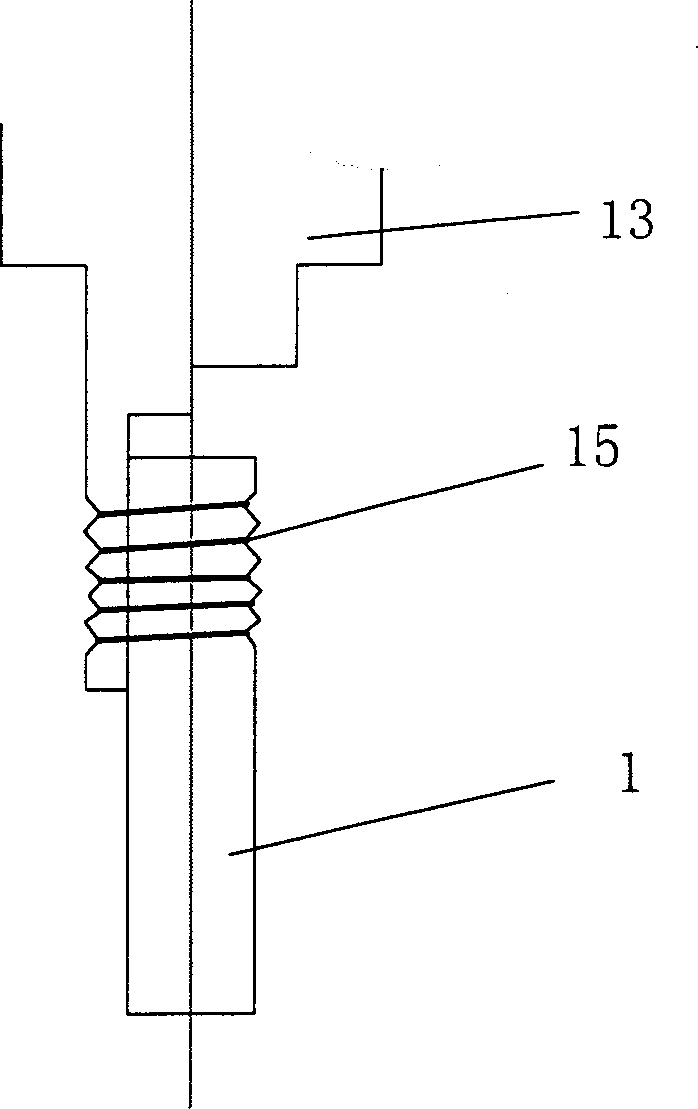
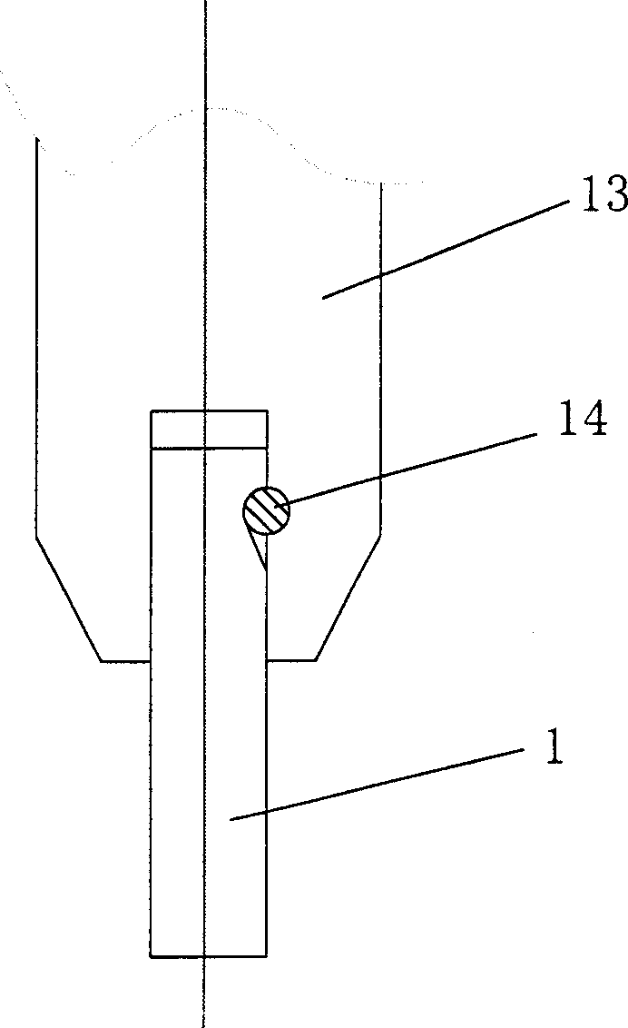
Image

Examples
Embodiment 1
[0050] Figure 4 It is a perspective view of a silicon seed crystal of the present invention. The silicon seed crystal of the present invention is divided into an upper part 1a of the silicon seed crystal and a lower part 1b of the silicon seed crystal, and the two parts are connected as a whole. The upper part 1a of the seed crystal is a rounded platform, the lower part 1b of the seed crystal is a cylinder, and the lower surface of the upper part 1a of the seed crystal is the upper surface of the lower part 1b of the seed crystal.
[0051] Figure 5 is a cross-sectional view of a seed crystal of the present invention. The angle θ between the sides of the rounded pedestal of the upper part 1a of the seed crystal and the axis is 15°.
[0052] The silicon seed crystal of the present invention is formed by cutting or drilling a silicon single crystal with a certain crystal orientation. The specific processing method is:
[0053] 1. Select a cylindrical silicon single crystal...
Embodiment 2
[0060] Figure 7 is a perspective view of another seed crystal of the present invention. The seed crystal of the present invention is divided into an upper part 1a of the silicon seed crystal and a lower part 1b of the silicon seed crystal, and the two parts are connected as a whole. The upper part 1a of the seed crystal is an inverted hexagonal prism, the lower part 1b of the seed crystal is a hexahedral prism, and the lower surface of the upper part 1a of the seed crystal is the upper surface of the lower part 1b of the seed crystal.
[0061] Figure 8 is a cross-sectional view of another seed crystal of the present invention. The included angle θ between the side edge and the axis of the inverted hexahedral prism at the upper part 1a of the seed crystal is 38°.
[0062] The silicon seed crystal of the present invention is formed by cutting or drilling a silicon single crystal with a certain crystal orientation. The steps that concrete processing method comprises are:
...
Embodiment 3
[0069] Figure 9 is a perspective view of another seed crystal of the present invention. The seed crystal of the present invention is divided into an upper part 1a of the silicon seed crystal and a lower part 1b of the silicon seed crystal, and the two parts are connected as a whole. The upper part 1a of the seed crystal and the lower part 1b of the seed crystal are truncated cones, and the cross section of the upper part 1a of the seed crystal is larger than the cross section of the lower part 1b of the seed crystal.
[0070] The silicon seed crystal of the present invention is formed by cutting or drilling a silicon single crystal with a certain crystal orientation. The steps that concrete processing method comprises are:
[0071] 1. Select a cylindrical silicon single crystal with a certain crystal orientation, with a diameter of 130 mm.
[0072] 2. Process it into strip-shaped cylinders on a drill press, each strip is 150 mm long. Diamond grains are plated on the stain...
PUM
| Property | Measurement | Unit |
|---|---|---|
| diameter | aaaaa | aaaaa |
| diameter | aaaaa | aaaaa |
Abstract
Description
Claims
Application Information