Semiconductor wafer protective member and semiconductor wafer grinding method

A technology for protecting components and single wafers, which is used in semiconductor/solid-state device manufacturing, workpiece support grinding, grinding/polishing equipment, etc., and can solve the problems of peeling off the protective tape, which are prone to cracks, fractures, and the peripheral part is not firmly fixed.

Inactive Publication Date: 2004-05-12
DISCO CORP
View PDF0 Cites 10 Cited by
  • Summary
  • Abstract
  • Description
  • Claims
  • Application Information

AI Technical Summary

Problems solved by technology

[0007] However, since the outer diameter of the semiconductor single wafer W1 (W2) is larger than the outer diameter of the suction area 71, there is no attractive force acting on the outer peripheral portion protruding from the suction area 71, so the outer peripheral portion is not firmly fixed.
Therefore, if grinding is performed in this state, there is a problem that the outer peripheral part is damaged due to continuous collisions, and thus cracks, notches, fractures, and other poor grinding occur.
[0008] Especially in the case of a thin semiconductor single wafer with a thickness of 100 μm or less, cracks are likely to occur when the protective tape is peeled off afterwards
This problem cannot be solved even if the protective tape T is made of highly rigid polyethylene terephthalate (PET) or the like.
[0009] In addition, in the case of so-called dicing first, the semiconductor single wafer in the outer peripheral portion is continuously hit, and the same problem as above occurs.

Method used


Image

  • Semiconductor wafer protective member and semiconductor wafer grinding method
  • Semiconductor wafer protective member and semiconductor wafer grinding method
  • Semiconductor wafer protective member and semiconductor wafer grinding method

Examples


Embodiment Construction

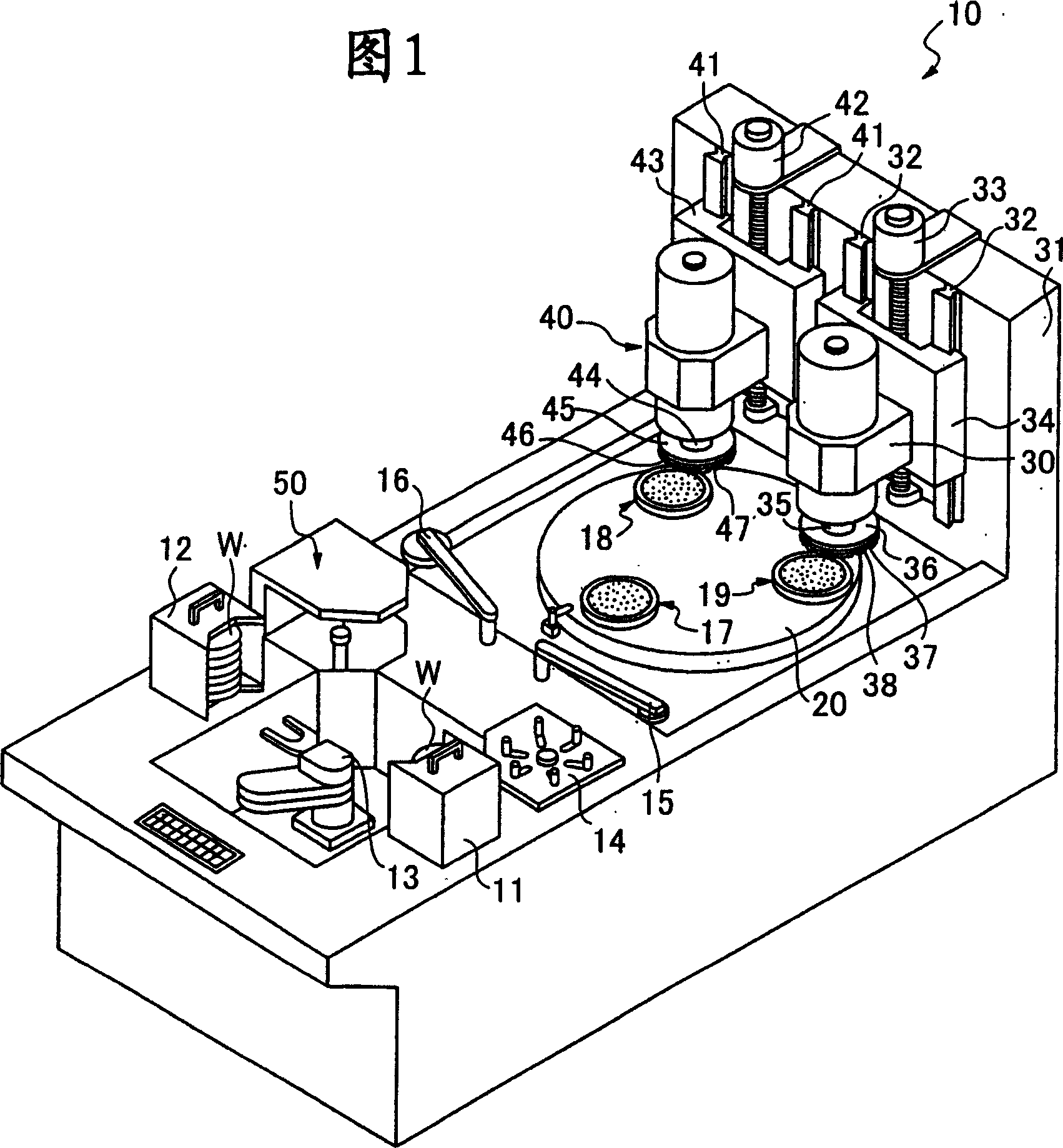
[0022] As an example of an embodiment of the present invention, a case where the back surface of a semiconductor single wafer is ground by the grinding apparatus 10 shown in FIG. 1 will be described.

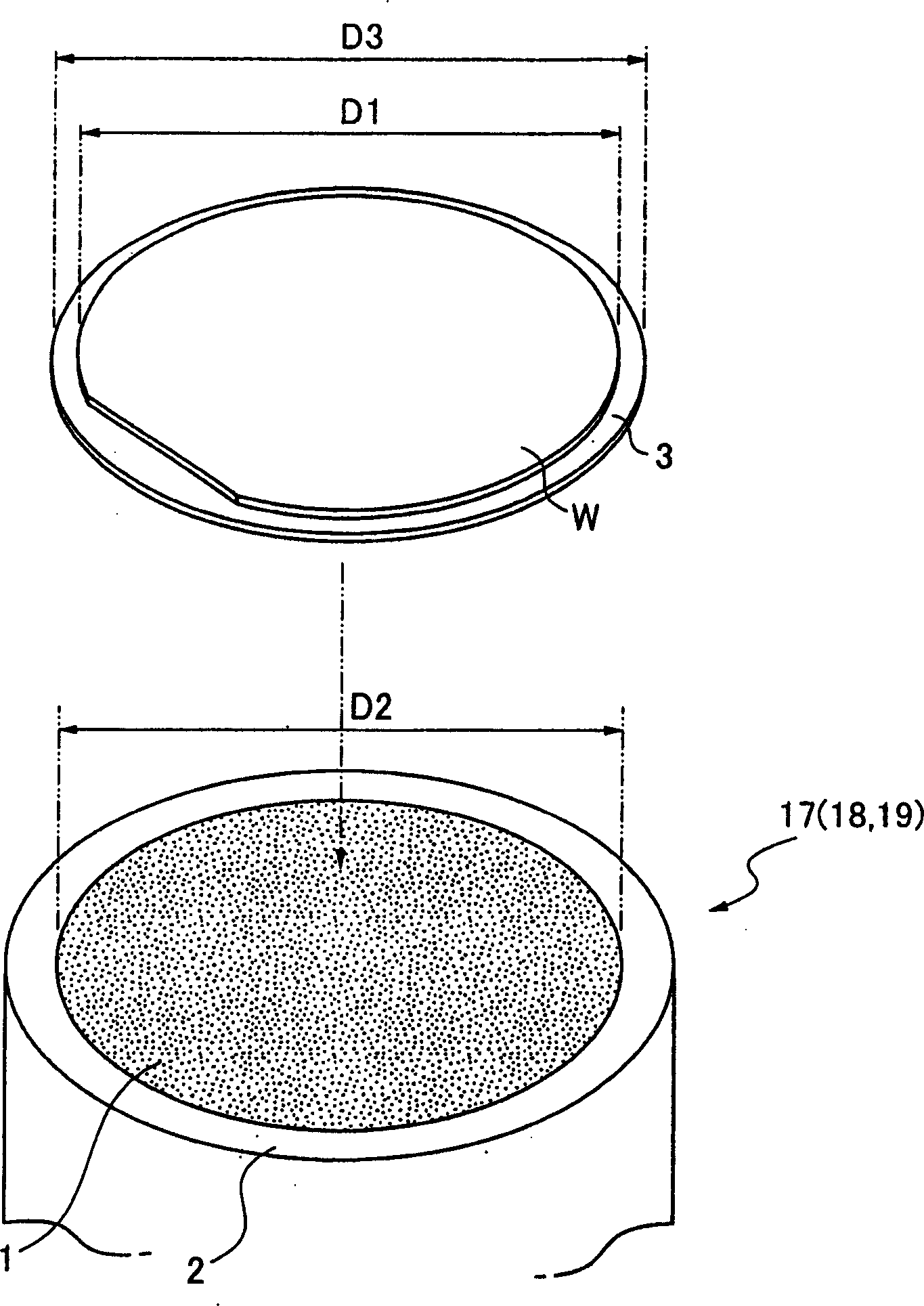
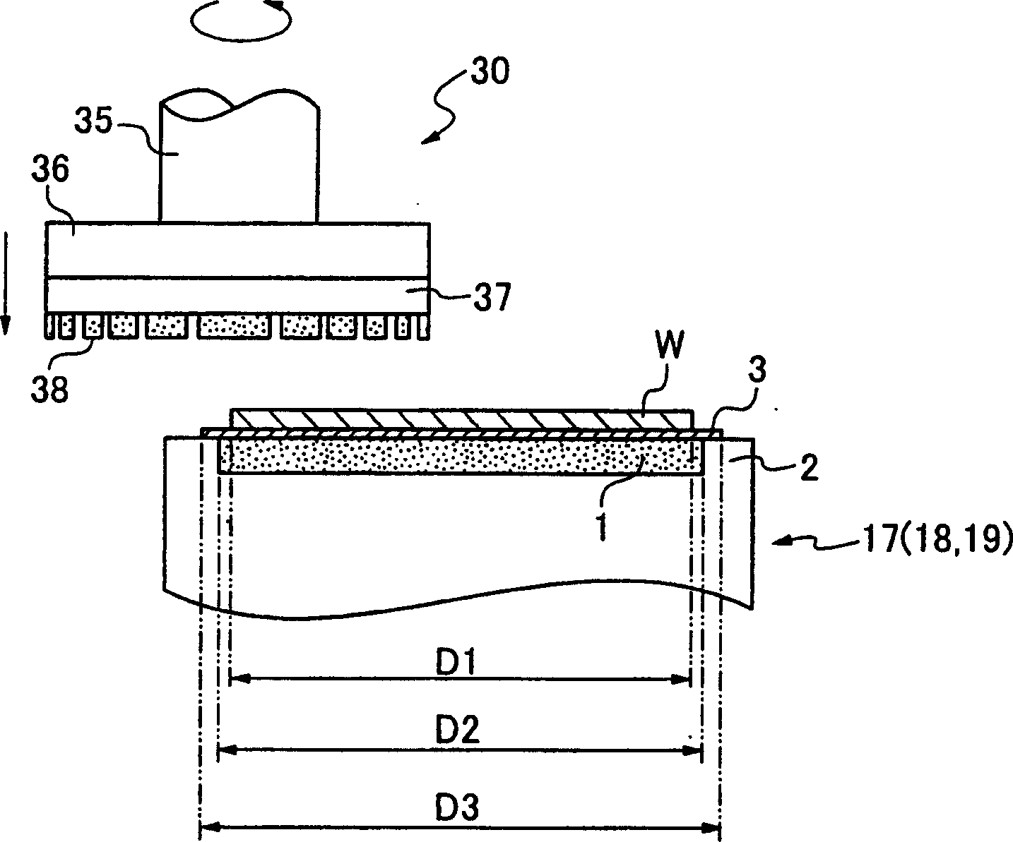
[0023] The grinding apparatus 10 includes: cassettes 11 and 12 for accommodating semiconductor single wafers W, and a carrying-in / out device 13 for carrying out semiconductor single wafers W from the cassettes 11 or carrying semiconductor single wafers W into the cassette 12, and performing grinding on the semiconductor single wafers W. The aligning device 14 for alignment, the first conveying device 15 and the second conveying device 16 for conveying the semiconductor single wafer W, the three suction cups 17 to 19 for attracting and holding the semiconductor single wafer W, and supporting the suction cups in a rotatable manner The turntable 20 rotating ground, the grinding units 30, 40 for grinding the semiconductor single wafer W held on each chuck, and the cleaning device 50 ...


PUM

PropertyMeasurementUnit
thicknessaaaaaaaaaa
thicknessaaaaaaaaaa

Abstract

A grinder composed of at least a chuck table (17) having a suction region (1) and a frame (2) and grinding means (30) for grinding a semiconductor wafer (W) held on the chuck table (17) is used. When a semiconductor wafer (W) having an outside diameter Dl smaller than that of the suction region (1) is ground, a semiconductor wafer (W) protective member (3) having an outside diameter D3 larger than the outside diameter Dl of the semiconductor wafer and larger than the diameter D2 of the suction region (1) is stuck on the side not to be ground of the semiconductor wafer (W). The whole surface of the semiconductor wafer (W) is held on the suction region (1), with the semiconductor wafer protective member (3) down. The exposed surface of the held semiconductor wafer (W) is ground by the grinding means (30). Thus the edge of the semiconductor wafer (W) is prevented from breaking, chipping and cracking.

Description

technical field [0001] The present invention relates to a protective member attached for surface protection when grinding a semiconductor single wafer, and a method of grinding a semiconductor single wafer using the protective member. Background technique [0002] Such as Figure 4 As shown, the semiconductor single wafer W1 divided by the separation strip S to form a plurality of integrated circuits (IC), large scale integration (LSI) and other circuits, after the backside is ground to a specified thickness, passes along the separation strip S. S performs vertical and horizontal cutting and each circuit is divided into individual semiconductor chips. [0003] Additionally, if Figure 5 As shown, the cutting groove 60 corresponding to the final thickness of the semiconductor chip is formed in advance on the separation zone S of the semiconductor single wafer W2, and the cutting groove 60 is exposed by grinding the backside thereof, and the pre-cutting of the individual semi...

Claims


Application Information

Patent Timeline
Patent Type & Authority Applications(China)
IPC IPC(8): B24B7/22B24B37/013C09J7/02C09J201/00H01L21/304H01L21/683
CPCH01L21/6838B24B7/228B24B41/06B24B37/04C09J201/00H01L21/304
Inventor 矢岛兴一木村祐辅
Owner DISCO CORP
Why Eureka
Try Eureka