

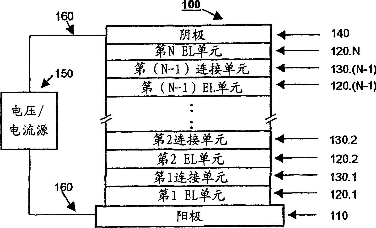
Cascade organic electroluminescence device with improved voltage stability
An electroluminescent device and electroluminescent technology, which are applied in electroluminescent light sources, electric light sources, electrical components, etc., can solve the problems of high light transparency, reduce device efficiency, and be difficult to obtain, so as to increase light output and reduce light loss, the effect of uncomplicated device structure
- Summary
- Abstract
- Description
- Claims
- Application Information
AI Technical Summary
Problems solved by technology
Method used
Image

Examples
Embodiment 1
[0128] Embodiment 1 (conventional OLED-comparative example)
[0129] The preparation of a conventional non-cascaded OLED was as follows: A - 1.1 mm thick glass substrate coated with a transparent ITO conductive layer was cleaned and dried with a commercial glass scrubbing tool. The thickness of ITO is about 42 nm and the sheet resistance of ITO is about 68Ω / square. The ITO surface was subsequently treated with an oxidizing plasma to the condition of the surface as an anode. by mixing CHF in an RF plasma chamber 3 A 1 nm thick layer of CFx was deposited on the clean ITO surface as the HIL. The substrate is then transferred to a vacuum deposition chamber for depositing all other layers on top of the substrate. by approximately 10 -6 The following layers were deposited in the following order by sublimation from a heated boat under a vacuum of Torr:
[0130] (1) HTL, 75nm thick, composed of NPB;
[0131] (2) ETL (also used as emission layer), 60nm thick, composed of Alq;
...
Embodiment 2
[0135] Embodiment 2 (comparative example)
[0136] The cascaded OLEDs were prepared as follows: A ~ 1.1 mm thick glass substrate coated with a transparent ITO conductive layer was cleaned and dried with a commercial scrubbing tool. The thickness of ITO is about 42nm and the surface resistance of ITO is about 68Ω / square. The ITO surface is then treated with an oxidizing plasma to the condition that the surface can serve as an anode. By decomposing CHF in an RF plasma processing chamber 3 gas to deposit a 1-nm-thick layer of CFx as HIL on a clean ITO surface. The substrate is then transferred to a vacuum deposition chamber for depositing all other layers on top of the substrate. by approximately 10 -6 The following layers were deposited in the following order by sublimation from a heated boat under a vacuum of Torr:
[0137] (1) HTL, 90nm thick, composed of NPB;
[0138] (2) ETL (also used as emission layer), 30nm thick, composed of Alq;
[0139] [NPB(90nm) / Alq(30nm), den...
Embodiment 3
[0150] Embodiment 3 (the present invention)
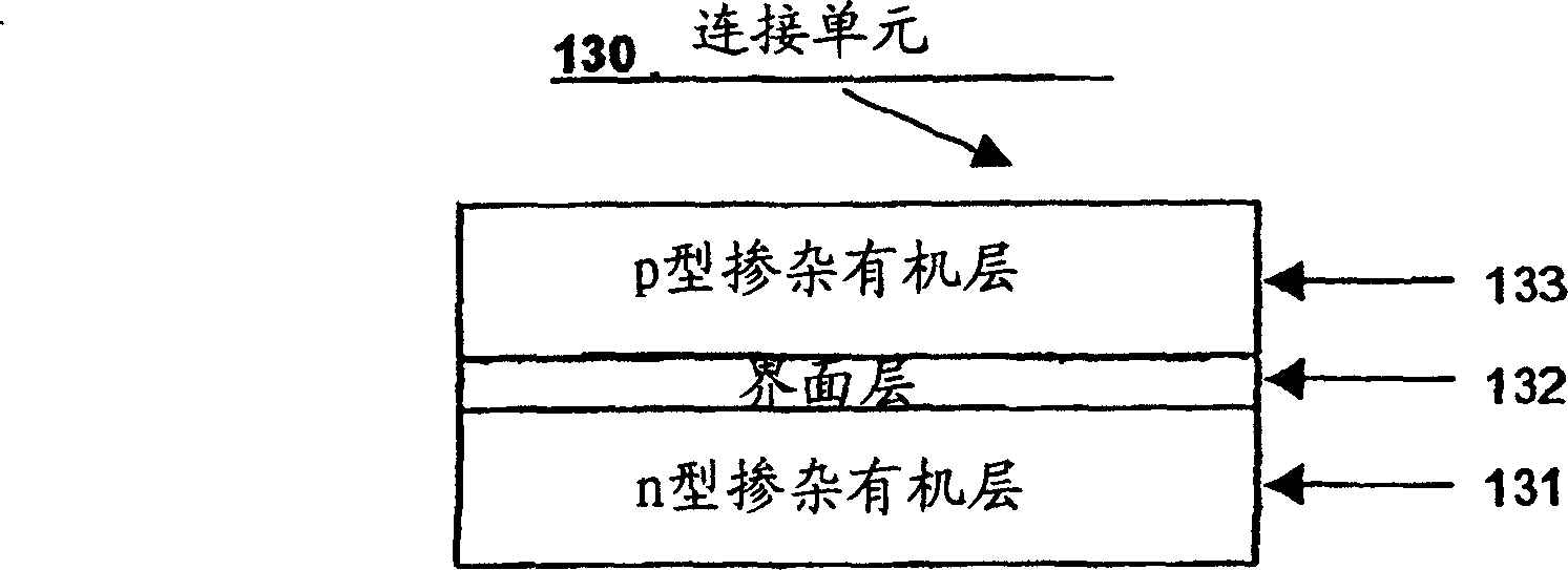
[0151] In addition to the Li-doped Alq layer in the junction unit with F 4 - A tandem OLED was manufactured in the same manner as in Example 2, except that 2 nm thick PbO was arranged between the TCNQ-doped NPB layers.
[0152] The cascaded device structure is denoted as ITO / CFx / EL1 / Alq:Li(30nm) / PbO(2nm) / NPB:F 4 -TCNQ(60nm) / EL2 / Mg:Ag.
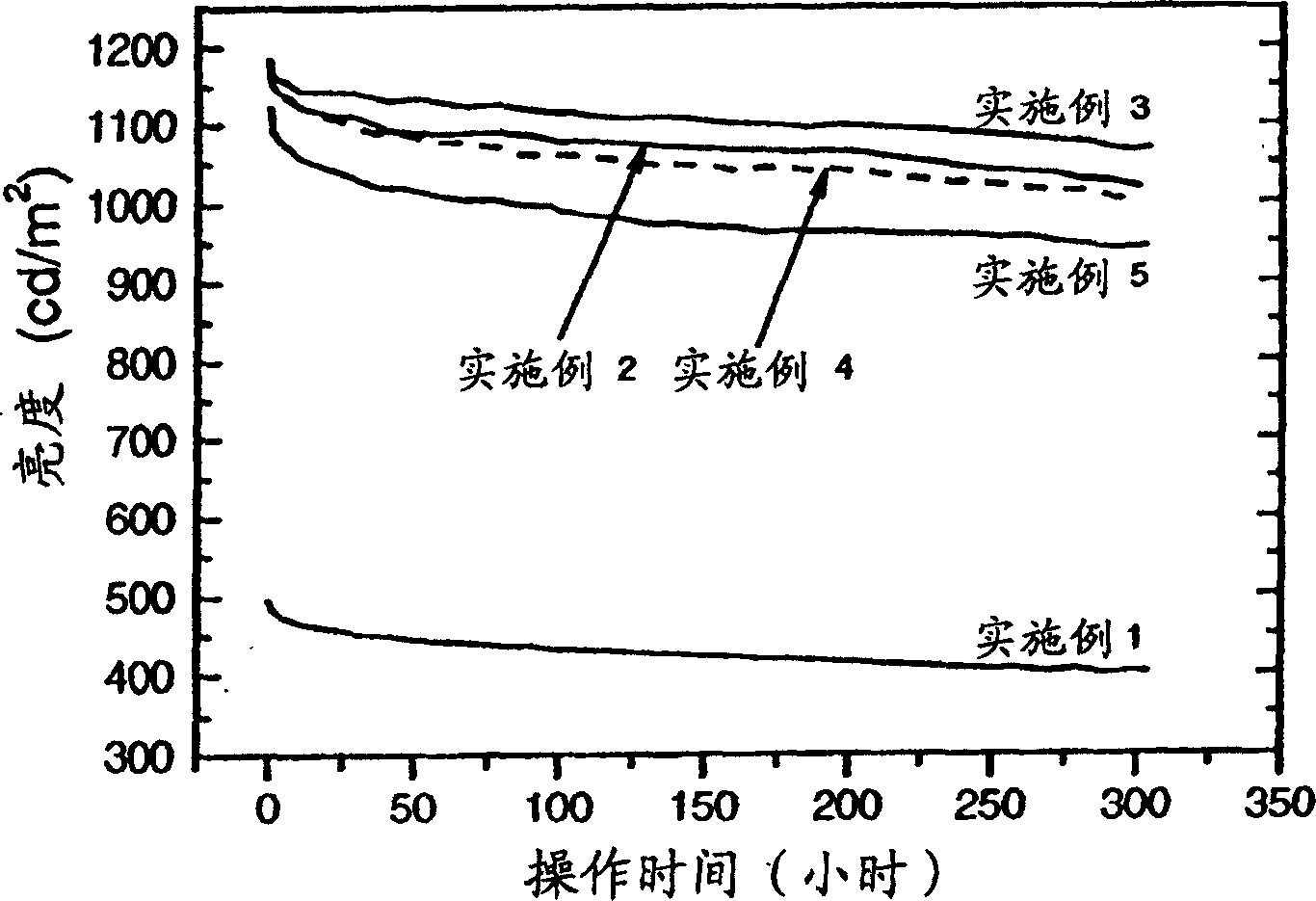
[0153] The cascaded OLED requires a 12.6V drive voltage to pass 20mA / cm 2 . Its brightness is 1177cd / m 2 And its luminous efficiency was about 5.9 cd / A, which were twice as high as the luminance and luminous efficiency in Example 1. exist image 3 The relationship between brightness decay and operating time is shown in . After 300 hours of operation, the brightness drops by about 10%. Figure 4 The voltage change versus operating time is shown in . The driving voltage was substantially unchanged after 300 hours of operation due to the insertion of a 2 nm thick PbO semiconductor interfacial ...
PUM
 Abstract
Description
Claims
Application Information