Method for preparing gallium nitride single crystal film

A single crystal thin film, trimethyl gallium technology, which is applied in the field of large mismatch epitaxial growth of III-N compound thin films, can solve the problems of limiting the optoelectronic properties of GaN single crystal thin films, unable to guarantee the best conditions for GaN growth, etc. Photoelectric properties, improving crystal quality, and suppressing the generation of crystal defects

Inactive Publication Date: 2004-06-02
INST OF PHYSICS - CHINESE ACAD OF SCI
View PDF0 Cites 21 Cited by
  • Summary
  • Abstract
  • Description
  • Claims
  • Application Information

AI Technical Summary

Problems solved by technology

The two-step growth method is to grow GaN under N-rich conditions. The problem is that the optimal conditions for GaN growth

Method used


Image

  • Method for preparing gallium nitride single crystal film
  • Method for preparing gallium nitride single crystal film
  • Method for preparing gallium nitride single crystal film

Examples


Embodiment 1

[0019] In this embodiment, a GaN single crystal film is epitaxially grown on a sapphire substrate. The method of the present invention will be described in detail below with reference to the drawings and embodiments:

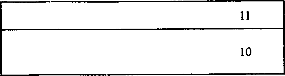
[0020] 1. First, clean the figure 1 The shown substrate 10 is placed on a substrate holder of a growth chamber in a chemical vapor deposition apparatus, hydrogen gas with a purity of 99.9999% is passed into the reaction chamber, and then the substrate is heated to 1200°C;

[0021] 2. Ten minutes later, lower the temperature of the substrate 10 to 400°C, pass ammonia and trimethylgallium carried by hydrogen into the reaction chamber, and keep the ammonia flow at 3000 or 8000 ml / min, trimethylgallium The flow rate is 1-10 ml / min to grow the nucleation layer 11 with a thickness of 1nm to 500nm. The nucleation layer 11 provides the core for the subsequent GaN growth, which plays a transitional role from the substrate to the GaN layer, and high-density nucleation The ce...

Embodiment 2

[0026] In this embodiment, a GaN single crystal thin film is epitaxially grown on a heterogeneous substrate.

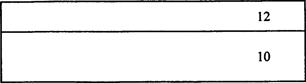
[0027] 1. First, clean the figure 1 The shown substrate 10 is placed on a substrate holder of a growth chamber in a chemical vapor deposition apparatus, hydrogen gas with a purity of 99.9999% is passed into the reaction chamber, and then the substrate is heated to 1200°C;

[0028] 2. After ten minutes, lower the temperature of the substrate 10 to between 500°C and 600°C, pass ammonia and trimethylgallium carried by hydrogen into the reaction chamber, and keep the ammonia flow at 5000-7000 ml / min , The trimethylgallium flow rate is 5-8 ml / min, to grow the nucleation layer 11 with a thickness of 100nm to 300nm. The nucleation layer 11 provides the core for the subsequent GaN growth and plays a transitional role from the substrate to the GaN layer. The high density of nucleation centers facilitates the subsequent growth of GaN;

[0029] 3. Stop feeding trimethylgallium into...


PUM


Abstract

The present invention is epitaxial growth method of monocrystal GaN film on heterogenous substrate. Monocrystal GaN film is grown on heterogenous substrate or sapphire substrate inside chemical vapor deposition apparatus. The growth process includes introducing hydrogen into reactor, heating the substrate to 1200; lowering the temperature after 10 min, leading in ammonia in the flow rate of 3000-8000 ml/min and hydrogen carried trimethyl gallium in the flow rate of 1-10 ml/min to grow GaN or AlN nucleating layer; in-situ annealing; maintaining substrate temperature at 700-1300 deg.c, leading trimethyl gallium into reactor to grow 1-500 nm GaN layer; lowering the molar V/III ratio to 0.5-2 and further growing GaN to 1-10000 nm thickness. The said process suppresses default generation, provides optimal monocrystal GaN film growing condition and thus has greatly raised crystal quality and photoelectronic characteristic.

Description

Technical field [0001] The invention relates to a method for growing a III-N compound film on a heterogeneous substrate with a large mismatch, in particular to a method for growing a GaN film on a heterogeneous substrate with a three-step growth method with a large mismatch. Background technique [0002] Wide band gap materials represented by III-N compounds such as GaN are the third-generation semiconductor materials after Si and GaAs and have received extensive attention. However, due to the limitations of GaN single crystal drawing technology, GaN-based films that are currently used in large numbers are grown on non-GaN substrates by epitaxial methods, using a two-step growth method, that is, nucleation layer growth at low temperature and GaN at high temperature. The layer grows normally. The specific operation is as follows: first grow a layer of 10-50nm GaN or AlN at 400-650°C, and then grow GaN at 900-1200°C after annealing at high temperature (900-1200°C). See: J. Cryst. G...

Claims


Application Information

Patent Timeline
IPC IPC(8): C30B25/02C30B29/38
Inventor 陈弘韩英军周均铭于洪波黄绮
Owner INST OF PHYSICS - CHINESE ACAD OF SCI
Why Eureka
Try Eureka