

A kind of conductive thin film and preparation method thereof
A technology of conductive film and inductive layer, which can be used in equipment for manufacturing conductive/semiconductor layers, cable/conductor manufacturing, conductive layers on insulating carriers, etc., and can solve problems such as poor conductivity of Ag-based conductive films
- Summary
- Abstract
- Description
- Claims
- Application Information
AI Technical Summary
Problems solved by technology
Method used
Image

Examples
Embodiment 1
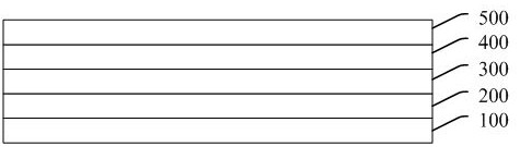
[0048] Using glass as the substrate, the glass was ultrasonically cleaned with deionized water, acetone, and ethanol for 15 minutes in advance to remove particles and organic pollutants on the substrate surface, and then dried with high-purity nitrogen to obtain a pretreated glass substrate ;
[0049] Spin-coat a layer of ZnO nanoparticle solution on the treated glass, and then heat at 80°C for 15 minutes to remove the solvent on the surface to form a ZnO layer with a thickness of 30nm;
[0050] Then spin-coat a layer of fullerene derivative PC at a concentration of 0.1 mg / mL on the ZnO layer. 61 BM solution, the solvent is chlorobenzene, and then heated at 80°C for 10 minutes to remove the solvent on the surface and form a PC with a thickness of 3nm 61 BM layer; then put the whole device into the vacuum evaporation chamber, and 61 A layer of Ag is vapor-deposited on the BM layer to form an Ag layer with a thickness of 3nm;
[0051] Finally, a layer of ZnO nanoparticle solu...
Embodiment 2
[0053] Using PEN as the substrate, the glass was ultrasonically cleaned with deionized water, acetone, and ethanol for 15 minutes in advance to remove particles and organic pollutants on the substrate surface, and then dried with high-purity nitrogen to obtain the pretreated PEN substrate ;
[0054] Spin-coat a layer of ZnO nanoparticle solution on the treated PEN, and then heat at 80°C for 15 minutes to remove the solvent on the surface to form a ZnO layer with a thickness of 30nm;
[0055] Then spin-coat a layer of fullerene derivative PC at a concentration of 0.1 mg / mL on the ZnO layer. 61 BM solution, the solvent is chlorobenzene, and then heated at 80°C for 10 minutes to remove the solvent on the surface and form a PC with a thickness of 3nm 61 BM layer; then put the whole device into the vacuum evaporation chamber, and 61 A layer of Ag is vapor-deposited on the BM layer to form an Ag layer with a thickness of 3nm;
[0056] Finally, a layer of ZnO nanoparticle solution...
Embodiment 3
[0058] Using glass as the substrate, the glass was ultrasonically cleaned with deionized water, acetone, and ethanol for 15 minutes in advance to remove particles and organic pollutants on the substrate surface, and then dried with high-purity nitrogen to obtain a pretreated glass substrate ;
[0059] Spin-coat a layer of Al-doped ZnO nanoparticle solution on the treated glass, and then heat at 80°C for 15 minutes to remove the surface solvent and form an AlZnO layer with a thickness of 30nm;
[0060] Then spin-coat a layer of fullerene derivative PC at a concentration of 0.1 mg / mL on the AlZnO layer. 61 BM solution, the solvent is chlorobenzene, and then heated at 80°C for 10 minutes to remove the solvent on the surface and form a PC with a thickness of 3nm 61 BM layer; then put the whole device into the vacuum evaporation chamber, and 61 A layer of Ag is vapor-deposited on the BM layer to form an Ag layer with a thickness of 3nm;
[0061] Finally, a layer of Al-doped ZnO ...
PUM
| Property | Measurement | Unit |
|---|---|---|
| thickness | aaaaa | aaaaa |
| thickness | aaaaa | aaaaa |
| concentration | aaaaa | aaaaa |
Abstract
Description
Claims
Application Information