A kind of aluminum nitride epitaxial structure and growth method thereof

An epitaxial structure and growth method technology, applied in the field of semiconductor light-emitting diodes, can solve problems such as difficulty in obtaining a smooth and flat AlN epitaxial layer, unfavorable lateral growth and merging of AlN epitaxial layers, etc., so as to improve internal quantum efficiency, promote lateral growth merging, and accelerate transformation effect

Active Publication Date: 2020-12-18
JIANGXI ZHAO CHI SEMICON CO LTD
View PDF9 Cites 0 Cited by
  • Summary
  • Abstract
  • Description
  • Claims
  • Application Information

AI Technical Summary

Problems solved by technology

Growth of AlN epitaxial layer on nano-patterned sapphire substrate (NPSS) can make up for the lack of lateral growth and migration ability of AlN. High temperature growth is conducive to two-dimensional growth of AlN, but AlN is easy to grow in the pit of NPSS during high temperature growth. It is not conducive to the lateral growth and merging of grid-like AlN epitaxial layers
And after growing AlN at a low temperature to form a three-dimensional shape, it directly enters the high-temperature growth stage, and it is difficult to obtain a smooth and flat AlN epitaxial layer.

Method used


Image

  • A kind of aluminum nitride epitaxial structure and growth method thereof
  • A kind of aluminum nitride epitaxial structure and growth method thereof
  • A kind of aluminum nitride epitaxial structure and growth method thereof

Examples


Embodiment 1

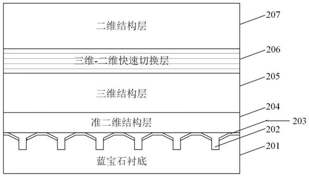
[0032] An embodiment of the present invention provides an aluminum nitride epitaxial structure, figure 1 A schematic structural diagram of an aluminum nitride epitaxial structure provided in this embodiment. see figure 1 , the aluminum nitride epitaxial structure sequentially includes a sapphire substrate 201, a nano-pattern array 202, an AlN nucleation layer 203, a quasi-two-dimensional structure layer 204, a three-dimensional structure layer 205, a three-dimensional-two-dimensional fast switching layer 206 and Two-dimensional structure layer 207 .

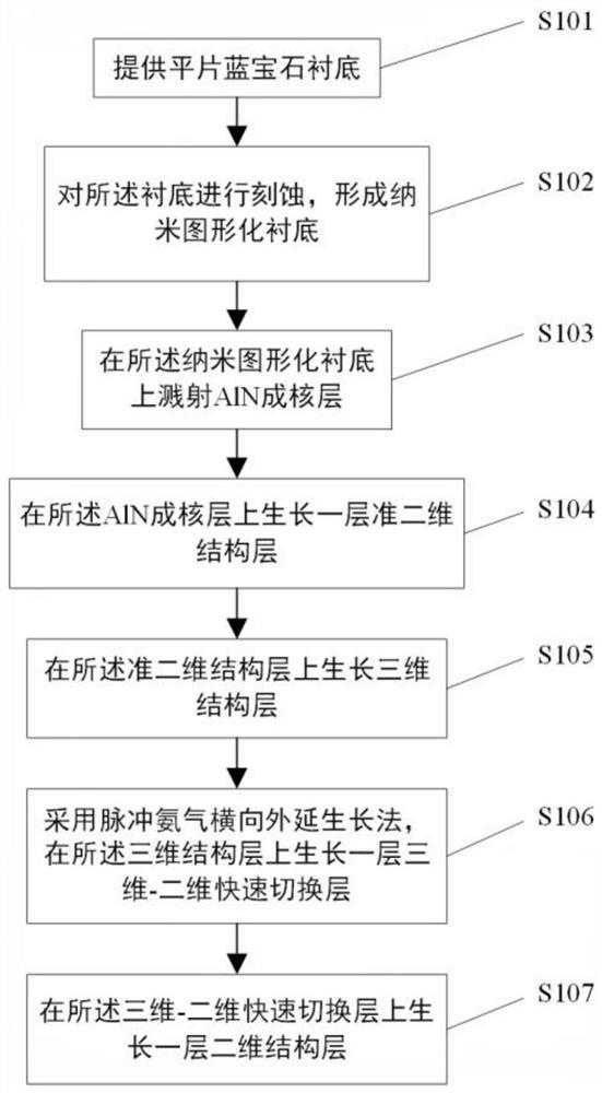
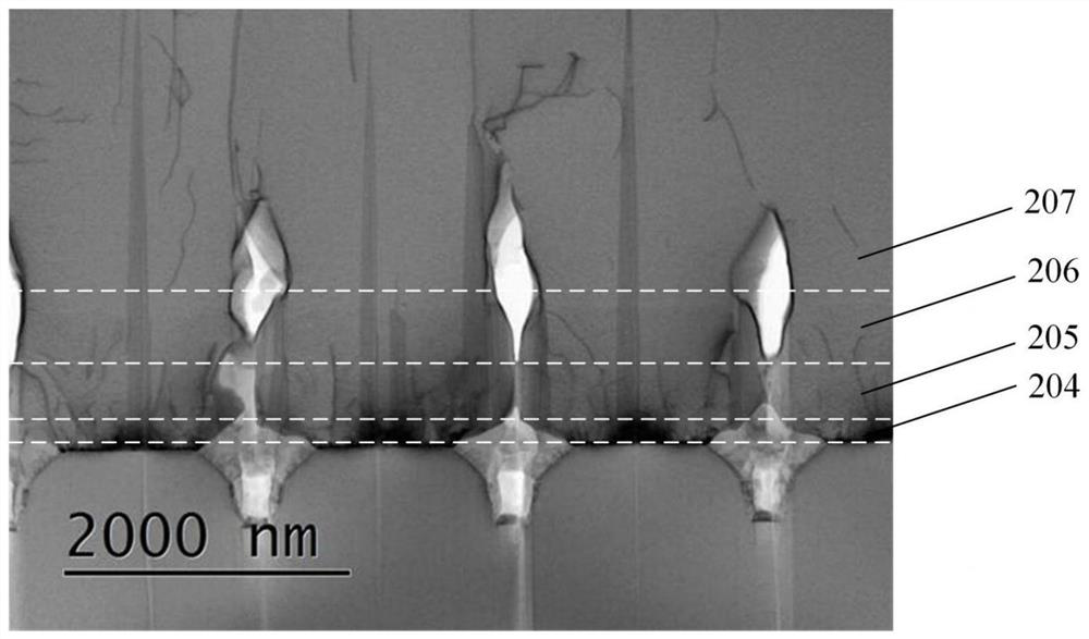
[0033] An embodiment of the present invention provides a method for growing an aluminum nitride epitaxial structure, figure 2 A flowchart of a method for growing an aluminum nitride epitaxial structure provided in this embodiment, image 3 A cross-sectional TEM image of an aluminum nitride epitaxial structure provided for an embodiment of the present invention, see figure 1 and image 3 , the production method includes: suc...

Embodiment 2

[0049] An embodiment of the present invention provides an aluminum nitride epitaxial structure, which sequentially includes a silicon carbide substrate 201, a nano-pattern array 202, an AlN nucleation layer 203, a quasi-two-dimensional structure layer 204, A three-dimensional structure layer 205 , a three-dimensional-two-dimensional fast switching layer 206 and a two-dimensional structure layer 207 .

[0050] An embodiment of the present invention provides a method for growing an aluminum nitride epitaxial structure, which specifically includes the following steps:

[0051] S101: providing a flat silicon carbide substrate 201;

[0052] S102: Etching the nano-pattern array 202 on the silicon carbide substrate 201;

[0053] Specifically, the nanopatterned array 202 is a pit-deep pit nanopattern array, and the specific structure is as follows Figure 4 As shown, the pit type is a rounded table pit 202-1 and a cylindrical deep pit 202-2, and the cylindrical deep pit 202-2 is etc...

Embodiment 3

[0066] An embodiment of the present invention provides an aluminum nitride epitaxial structure, which sequentially includes a silicon substrate 201, a nano-pattern array 202, an AlN nucleation layer 203, a quasi-two-dimensional structure layer 204, a three-dimensional Structure layer 205 , 3D-2D fast switching layer 206 and 2D structure layer 207 .

[0067] An embodiment of the present invention provides a method for growing an aluminum nitride epitaxial structure, which specifically includes the following steps:

[0068] S101: providing a flat silicon substrate 201;

[0069] S102: Etching the nano-pattern array 202 on the silicon substrate 201;

[0070] Specifically, the nanopatterned array 202 is a pit-deep pit nanopattern array, and the specific structure is as follows Figure 4 As shown, the pit type is a rounded table pit 202-1 and a cylindrical deep pit 202-2, and the cylindrical deep pit 202-2 is etched at the bottom of the rounded bench pit 202-1. The pattern period...


PUM

PropertyMeasurementUnit
thicknessaaaaaaaaaa
thicknessaaaaaaaaaa
thicknessaaaaaaaaaa

Abstract

The invention discloses an aluminum nitride epitaxial structure. The structure comprises a nano patterned sapphire substrate, an aluminum nitride (AlN) nucleating layer, a quasi-two-dimensional structure layer, a three-dimensional structure layer, a three-dimensional-to-two-dimensional rapid switching layer and a two-dimensional structure layer, wherein the quasi-two-dimensional structure layer isa 2D-morphology aluminum nitride layer of a net structure, the three-dimensional structure layer is a 3D-morphology aluminum nitride layer, the three-dimensional-to-two-dimensional rapid switching layer is a 2D-morphology aluminum nitride layer, and the two-dimensional structure layer is a 2D-morphology aluminum nitride layer. The invention further provides a growth method of the aluminum nitrideepitaxial structure. In an AlN epitaxial growth process, an AlN epitaxial layer with a smooth and flat surface can be obtained by adopting a high temperature-low temperature-pulsed ammonia gas-high temperature four-step growth method and through regulating and controlling temperature and V / III in the AlN growth process and on the basis of a pulsed ammonia gas lateral epitaxial growth technology,and therefore, the dislocation density of the epitaxial layer is effectively reduced, the crystal quality of the AlN epitaxial layer is improved, and the internal quantum efficiency of an ultravioletlight-emitting diode is improved.

Description

technical field [0001] The invention relates to the technical field of semiconductor light-emitting diodes, in particular, the invention relates to an aluminum nitride epitaxial structure and a growth method thereof. Background technique [0002] Aluminum nitride (AlN) has the advantages of high band gap, high thermal conductivity and strong radiation resistance, and is widely used in ultraviolet light-emitting diode (UV LED) devices. Since the lattice constant and thermal expansion coefficient of AlN crystal and GaN crystal are relatively close, the lattice mismatch between sapphire and gallium nitride (GaN) materials can be reduced, and the crystal quality of epitaxially grown AlGaN can be improved, thereby improving the photoelectric performance of UV LEDs. However, the lattice constant and thermal expansion coefficient of the sapphire substrate and the AlN material are large, and there is still a large lattice mismatch, which will introduce a large dislocation density an...

Claims


Application Information

Patent Timeline
Patent Type & Authority Patents(China)
IPC IPC(8): H01L33/12H01L33/32H01L33/00C30B25/04C30B25/06C30B29/40
CPCC30B25/04C30B25/06C30B29/403H01L33/007H01L33/12H01L33/32
Inventor 周圣军宫丽艳胡红坡万辉
Owner JIANGXI ZHAO CHI SEMICON CO LTD
Why Eureka
Try Eureka