
Carbon nanometer tube array structure and growing method thereof

A carbon nanotube array, carbon nanotube technology, applied in nanotechnology, nanotechnology, nanotechnology for information processing, etc., can solve the problem of increasing the complexity of device design, difficult to achieve local multiple growth direction control, and limiting carbon Diversification and practicability of nanotube devices to achieve the effect of rich diversity and multiple choice spaces

Inactive Publication Date: 2004-07-07
TSINGHUA UNIV +1
View PDF0 Cites 56 Cited by
  • Summary
  • Abstract
  • Description
  • Claims
  • Application Information

AI Technical Summary

Problems solved by technology

[0007] However, in the above methods, the method of using electric field to control the growth direction of carbon nanotubes will increase the complexity of device design, and because of the wide area of ​​the electric field itself, it is difficult to realize the control of multiple local growth directions.
These factors limit the diversification and practicability of carbon nanotube device design. Therefore, it is necessary to develop a local carbon nanotube growth direction control method that does not require an external field.

Method used


Image

  • Carbon nanometer tube array structure and growing method thereof
  • Carbon nanometer tube array structure and growing method thereof
  • Carbon nanometer tube array structure and growing method thereof

Examples


Embodiment Construction

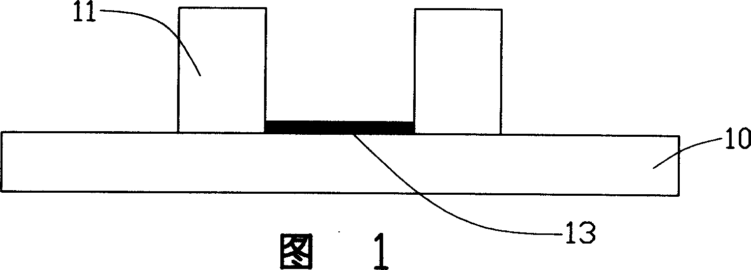
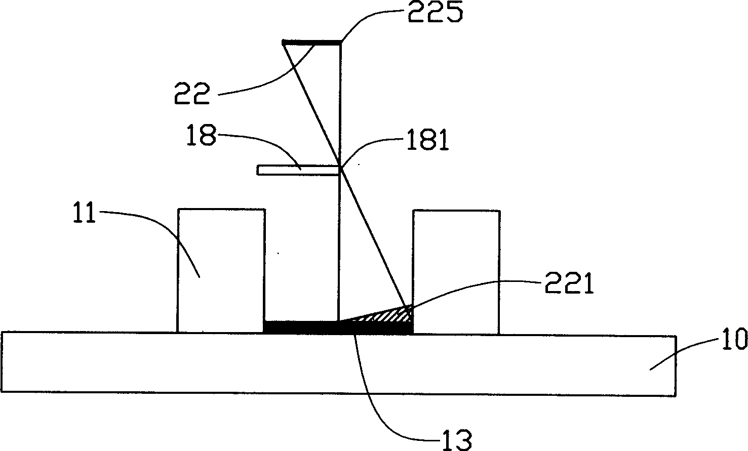
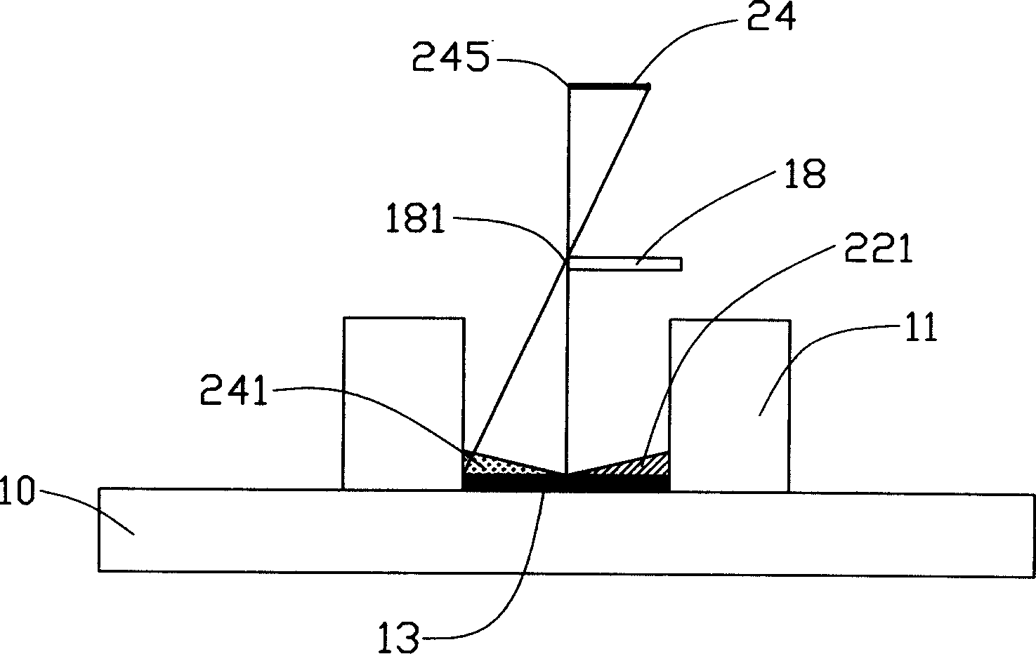
[0029] Referring to FIG. 1 , firstly, a substrate 10 is provided, and the substrate 10 is made of silicon, and a photoresist 11 is formed on the substrate 10 , and the photoresist 11 is formed into a predetermined pattern by photolithography. Deposit a catalyst 13 with a thickness of several nanometers at the position where carbon nanotubes need to be grown. The deposition method of the catalyst 13 can be thermal evaporation deposition method, or electron beam heating evaporation method and other methods can be used to cooperate with the photolithography process or pattern mask. The catalyst 13 The thickness is at least 2 to 3 nanometers, at most 10 nanometers, and the thickness needs to be uniform. The material can be iron, cobalt, nickel or their alloys. In the first embodiment, iron is selected as the material of the catalyst 13, and the deposited thickness is 6 nanometers.

[0030] see figure 2 , deposit a layer of regulating material 221 that affects the growth rate of c...


PUM


Abstract

A carbon nanotube array structure is composed of a substrate, the alloy catalyst particles on the substrate, which contains the material to affect the growth speed of carbon nanotubes, and the array the carbon nanotubes which is grown from said alloy catalyst particles and bent toward a predefined direction. Its growing process includes such steps as generating a catalyst layer on the substrate, depositing at least two kinds of growth speed regulating material, annealing in oxygen contained gas to change the catalyst layer to catalyst particles, introducing carbon source gas, and growing carbon nanotubes.

Description

【Technical field】 [0001] The invention relates to a carbon nanotube array structure and a growth method thereof. 【Background technique】 [0002] Due to the unique electrical properties of carbon nanotubes, their applications in the fields of nano-integrated circuits and single-molecule devices have immeasurable prospects. At present, people have been able to manufacture a small amount of carbon nanotube-based field effect transistors, logic devices, and storage devices in the laboratory, and have studied its properties. For details, please refer to Sander J Tans et al. published in Nature 393-49 in 1998, Room-temperature transistor based on a single carbon nanotube article. But for large-scale preparation and practical application, we must resort to bottom-up (Bottom Up) preparation process. [0003] The bottom-up preparation process requires the ability to control the growth position, direction, size, length, and even the helicity of carbon nanotubes, and directly grow th...

Claims


Application Information

Patent Timeline
Patent Type & Authority Applications(China)
IPC IPC(8): D01F9/127
CPCB82Y10/00D01F9/127B82Y30/00Y10T428/30
Inventor 刘亮范守善
Owner TSINGHUA UNIV
Learn More