Method for making optically-controlled transistor and its structure

A manufacturing method, transistor technology, applied in the direction of final product manufacturing, sustainable manufacturing/processing, semiconductor devices, etc.

Inactive Publication Date: 2004-07-28
VTERA TECH
View PDF1 Cites 5 Cited by
  • Summary
  • Abstract
  • Description
  • Claims
  • Application Information

AI Technical Summary

Problems solved by technology

However, HEMT transistors still use the gate to control the drain current. In the design of photoelectric transistors in general optoelectronic components, this 2DEG characteristic cannot be applied.

Method used


Image

  • Method for making optically-controlled transistor and its structure
  • Method for making optically-controlled transistor and its structure
  • Method for making optically-controlled transistor and its structure

Examples


Embodiment Construction

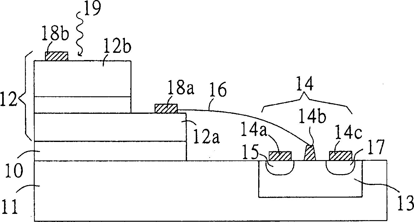
[0038] As mentioned above, in order to form a prism-shaped light-receiving layer between the source and drain of the transistor, the feature of the present invention is to grow a layer of boron phosphide (BP) as a buffer layer on the silicon substrate, and then continue By growing gallium nitride-based materials, it is possible to form a gallium nitride-based layer with a cubic lattice (Cubic Lattice). Since the cubic lattice has and crystal planes, it is easy to form such a layer by epitaxy or etching. The prism-shaped light-receiving layer can therefore improve the light-controlling sensitivity of the transistor of the present invention.

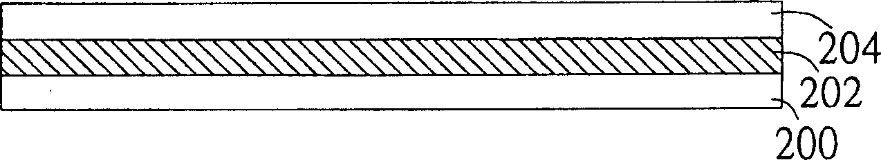
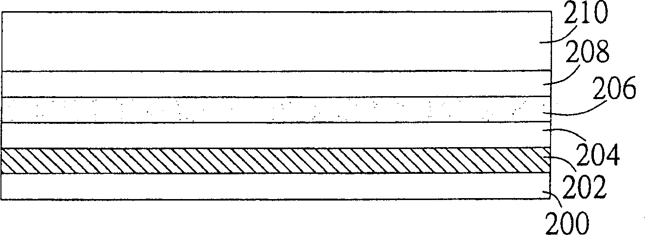
[0039] Please refer to Figure 2A, in order to form gallium nitride-based materials with a cubic lattice, the phototransistor of the present invention forms a buffer layer 202 of boron phosphide material on the surface of the crystal plane of the silicon substrate 200, and then forms a layer aluminum nitride (AlN) layer 204 . Wherein ...


PUM

PropertyMeasurementUnit
thicknessaaaaaaaaaa
electron mobilityaaaaaaaaaa

Abstract

The invention discloses a phototransistor making method and structure, firstly forming a boron phosphide buffer layer on the silicon substrate, then forming the first aluminium nitride to compensate stress, then forming the gallium nitride layer and n-type aluminium nitride layer as the heterogenous junction, then making selective extension or anisotropic etching on the gallium nitride material to form prism shaped light accepting layer with cubic crystal lattice, wherein the light accepting layer gathers the incident light beam to excite the electrons in the n-type aluminium nitride layer and forming high-speed two dimensional electron current in the gallium nitride layer, heightening the power and sensitivity of the phototransistor.

Description

technical field [0001] The present invention relates to a method for manufacturing a phototransistor and its structure, and in particular to a method of forming a prism-shaped light-receiving layer between a source electrode and a drain electrode to replace a gate electrode. ) electrode phototransistor manufacturing method and its structure. Background technique [0002] In the 21st century, the information society has entered the terabit era. Optoelectronics technology plays a key role in the transmission, processing, storage and display of megabit information, and the Optoelectronic Integrated Circuit (OEIC) is a centralized design of multiple optical components and electronic components. The process technology on the same substrate has become a technology with great development potential in optoelectronic technology because it can reduce the size of components, reduce manufacturing costs, and increase operational stability. [0003] Please refer to figure 1 , which is ...

Claims


Application Information

Patent Timeline
Patent Type & Authority Applications(China)
IPC IPC(8): H01L31/10H01L31/18
CPCY02P70/50
Inventor 寺嶋一高徐顺弘章烱煜赖穆人
Owner VTERA TECH
Why Eureka
Try Eureka