
Technical method for integrated circuit design, test and measurement integration

A technology of integrated circuits and technologies, applied in circuits, electrical solid state devices, computing, etc., to achieve the effect of improving design accuracy and use efficiency

Inactive Publication Date: 2004-08-18
上海芯华微电子有限公司 +2
View PDF0 Cites 43 Cited by
  • Summary
  • Abstract
  • Description
  • Claims
  • Application Information

AI Technical Summary

Problems solved by technology

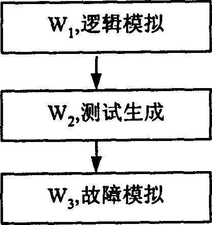
This technology has not fundamentally involved verification techniques such as geometrical design rule checking (DRC), circuit logic consistency checking (LVS), and testing techniques such as test generation and fault simulation

Method used


Image

  • Technical method for integrated circuit design, test and measurement integration
  • Technical method for integrated circuit design, test and measurement integration
  • Technical method for integrated circuit design, test and measurement integration

Examples


Embodiment Construction

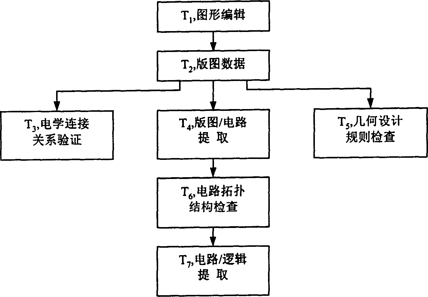
[0035] The method of the present invention is realized by computer program control, and consists of three parts: the design of the integrated circuit; the verification of the integrated circuit; and the test of the integrated circuit.

[0036] Part I: Integrated Circuit Design.

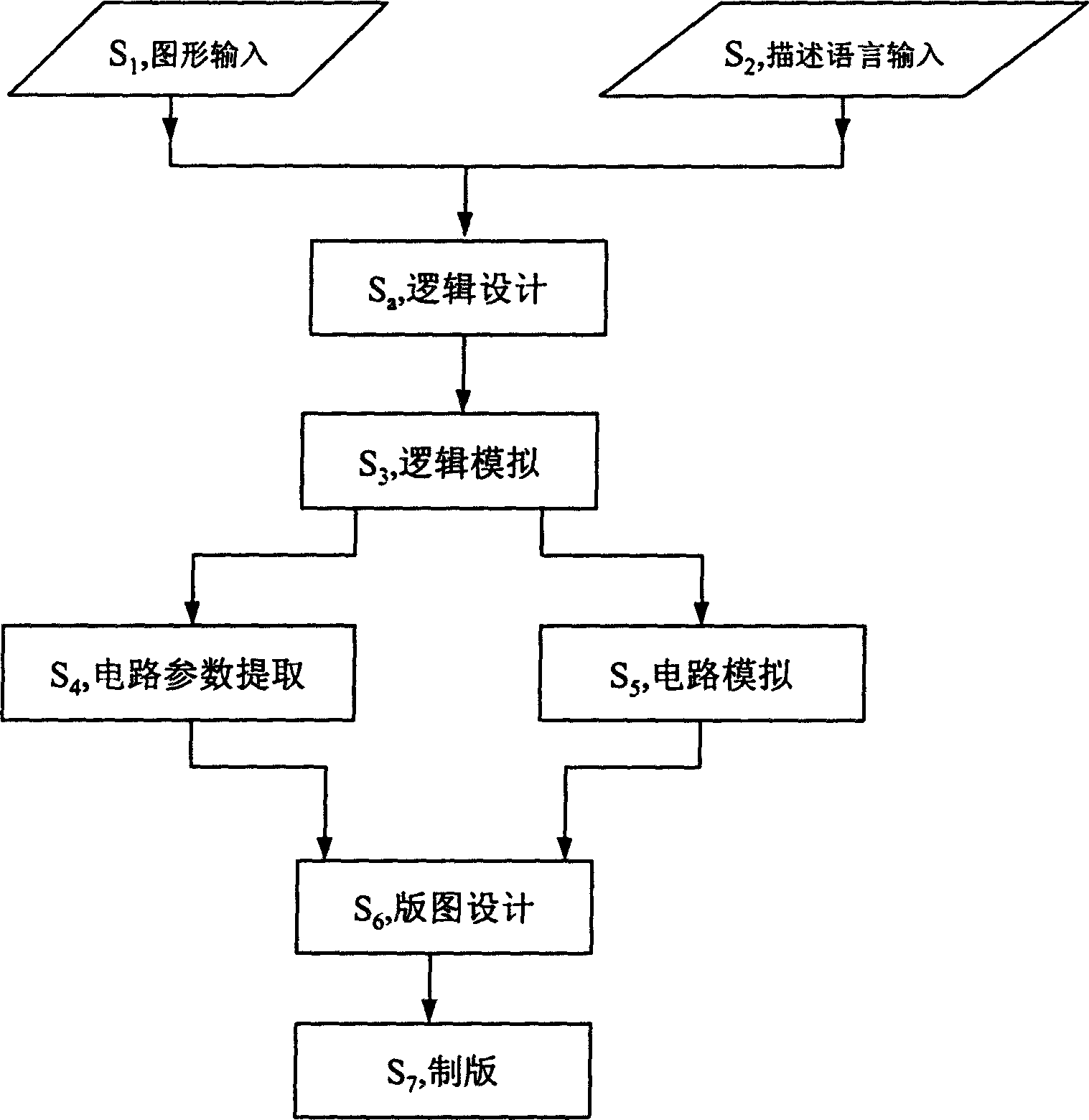
[0037] For ease of presentation, this part of the invention is referred to as an automatic design subsystem, see figure 1 , figure 1 It is a block diagram of the automatic design subsystem in integrated circuit design. The entire automatic design subsystem is divided into: (1) input form of integrated circuit design subsystem; (2) logic design; (3) logic simulation; (4) circuit parameter extraction and circuit simulation; (5) layout design; (6) plate making.

[0038] The workflow of automatic design subsystem is as follows:

[0039] S 1 , the step of graphic input is used to input the design information of the integrated circuit, and the form of graphic input can provide the user with a means of i...


PUM


Abstract

The invention relates to an integration circuit design, checking and testing integrated process which is realized by a computer-controlled integral system comprising, an automation design subsystem for presenting the key technical points of each steps from design input to printing chart, a verification subsystem for presenting rule inspection from electricity connected relation checking to geometry design and verification each key technical points, and a testing subsystem for presenting key points of testing survival and fault simulation.

Description

(1) Technical field [0001] The present invention belongs to the fields of integrated circuit design technology, verification technology and testing technology, and in particular refers to a technical method integrating the three to form a integrated circuit design, verification and testing centered on a unified database. (2) Background technology [0002] Integrated circuit design-verification-testing technology (Design-verification-testing technology for integrated circuits) is a new technology that integrates integrated circuit design technology, verification technology and testing technology. Its main body is the design technology of VLSI. When the integrated circuit develops to the very large scale (VLSI) stage, because the integration level of the circuit is greatly improved, the complexity of the circuit increases sharply, and each step of the design must be accompanied by effective verification. In this case, the design and verification of integrated circuits must be...

Claims


Application Information

Patent Timeline
IPC IPC(8): G06F17/50H01L21/82H01L27/00
Inventor 林争辉林涛戎蒙恬王海雄陈艳
Owner 上海芯华微电子有限公司
Learn More