High power LED

A light-emitting diode, high-power technology, applied in electrical components, electric solid-state devices, circuits, etc., can solve the problems of large thermal resistance, small metal base area, overheating of light-emitting diodes, etc. handy effect

Inactive Publication Date: 2004-11-10
浙江城建建设集团有限公司
View PDF0 Cites 22 Cited by
  • Summary
  • Abstract
  • Description
  • Claims
  • Application Information

AI Technical Summary

Problems solved by technology

The area of ​​the metal base is small, for example, less than 6mm in diameter, and the thermal conductivity of aluminum is only about 1/2.5 of that of copper. The copper heat conduction adhesive layer has a large thermal resistance, and t

Method used


Image

  • High power LED
  • High power LED
  • High power LED

Examples


Example Embodiment

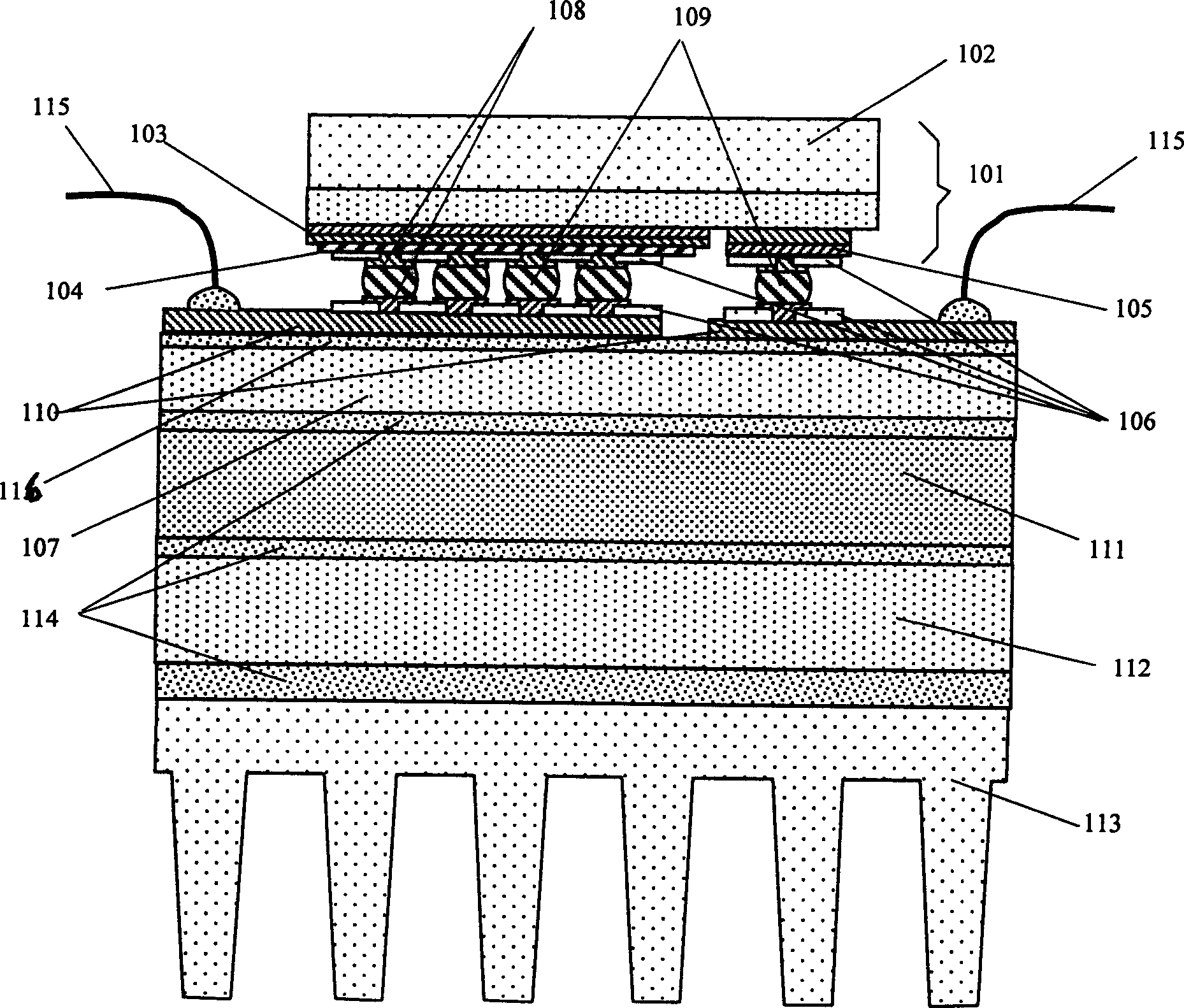
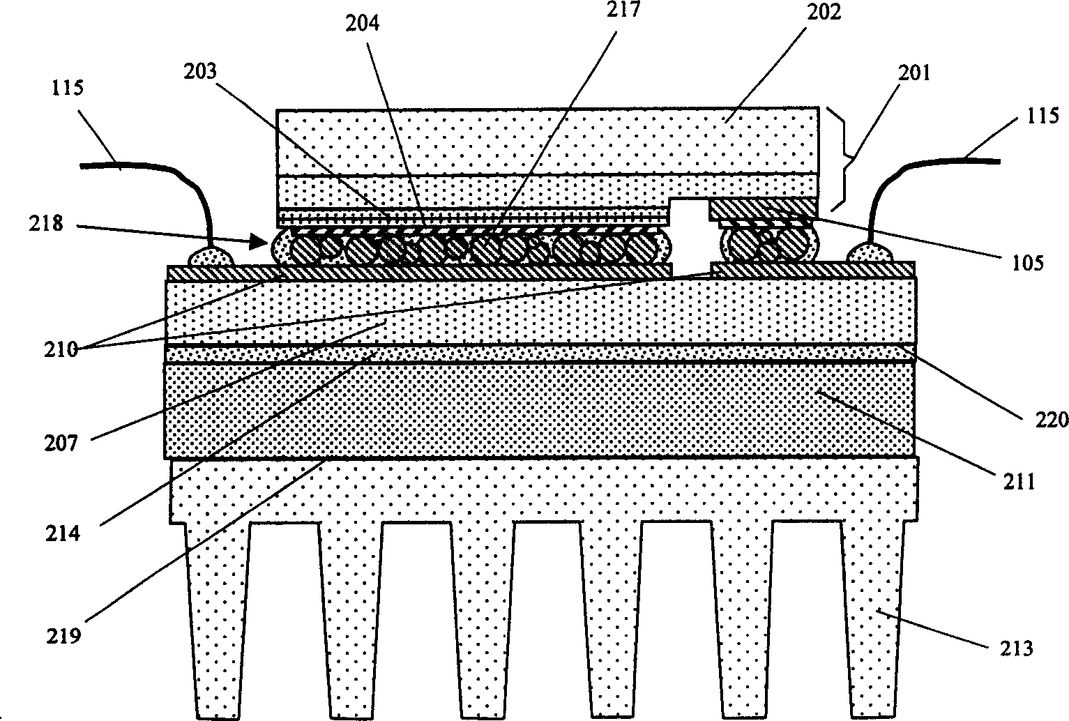
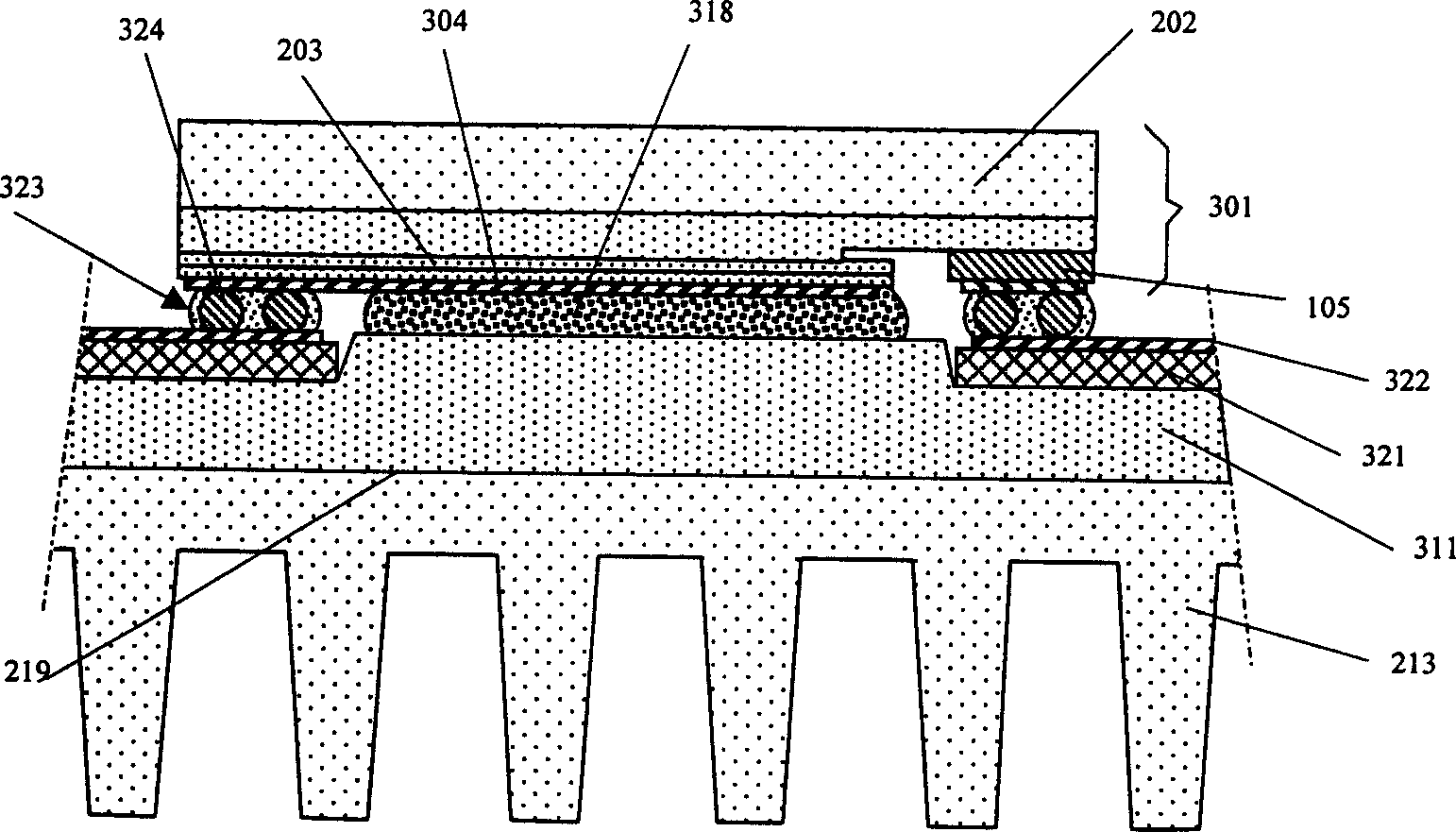
[0024] The present invention mainly includes at least one light-emitting diode chip, and the light-reflective metal electrode on the outer surface of the pn junction of the chip is mounted on a silicon substrate with a higher thermal conductivity than a silicon substrate through self-localized solder mixed with small silver beads or small gold beads. On a diamond substrate; the self-localized solder mixed with small silver beads or small gold beads is adsorbed by the small silver beads or small gold beads when the solder is melted, and will not flow out to cause short circuit of the electrode, that is, no dielectric layer is needed at the welding place. Self-localization, while its thickness can be controlled by the diameter of small silver beads or small gold beads, its thickness can be very thin, such as less than 0.04mm, and the contact area with the chip can be large, such as greater than 30% of the chip area; the diamond substrate There is a solderable circuit conductive laye...


PUM

PropertyMeasurementUnit
Thicknessaaaaaaaaaa

Abstract

The invention is a high-power light-emitting diode (LED), at least including a LED chip, optical refection metallic electrodes on the outer surface of the p-n junction are directly mounted on a metallic base through high thermal conductivity material or diamond whose thermal conductivity is thrice higher than that of Cu, where the high thermal conductivity material can be small-Ag/Au pearl mixed soldering tin, diamond thermal conducting glue or Ag pearl/powder mixed thermal conducting glue; the electrodes are led out from the conductive layer or circuit board of a diamond basal plate, and the metallic base has at least one screw or screw hole used in connection with cooler; the chip and metallic base have transmitting mediums and lenses, and lighting material also, and the chip can be used for making LED lamps, solar energy LED lamps, LCD back lighting, information display, etc.

Description


Claims


Application Information

Patent Timeline
Owner 浙江城建建设集团有限公司
Why Eureka
Try Eureka